Society realized by Industrial Equipment Business
Nanoimprint opens
a new door to the future of digital society

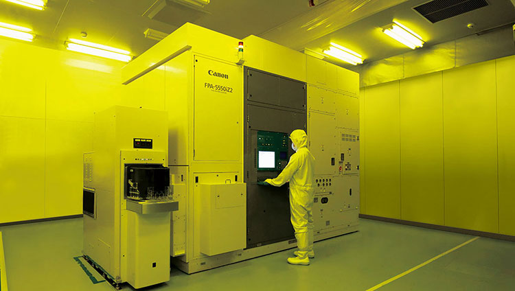
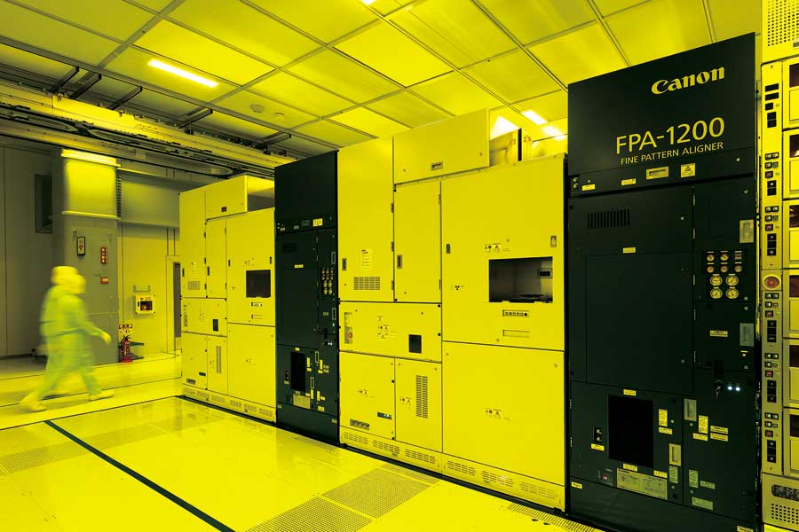
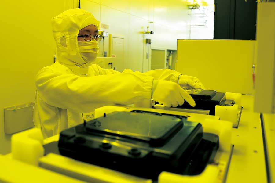
Located in western Japan, Toshiba Memory Corporation's Yokkaichi Operations plant stands at the forefront of semiconductor memory production. Here, verification is underway for the application of Canon's nanoimprint technology for the mass production of semiconductor devices. The miniaturization of circuit patterns has brought dramatic improvement to semiconductor memory performance and capacity. In recent years, however, the conventional approach of using light to transfer the circuit patterns onto chips appears to be approaching a technological limit. To overcome this hurdle to further miniaturization, Canon has developed semiconductor lithography equipment that employs an innovative approach called nanoimprint lithography, which is gaining recognition not only for its nano-level precision, but also for the relative compactness of the equipment used, which can significantly reduce semiconductor manufacturing costs.
Using nanoimprint technology to manufacture next-generation flash memory
With the advent of the age of the Internet of Things (IoT), where everything will be connected to the internet, all kinds of objects will be equipped with such semiconductor devices as sensors and communication devices, memory for data storage and processors for AI that analyze big data. Demand is ever increasing for these semiconductor devices as they become even more vital to society.
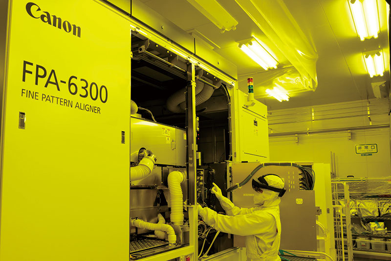
Semiconductor devices evolve through miniaturization, or narrowing the circuit line widths and increasing the density of circuit patterns on the device. Advances in semiconductor lithography equipment are the key to achieving this miniaturization and reducing manufacturing costs. Conventionally, miniaturization was achieved by shortening the wavelength of the light source used when exposing the device. The technological limit of this method, however, appears to have been reached, making an innovative new approach necessary.
Canon, together with Canon Nanotechnologies, has developed a method that eliminates the projection lens used to reduce and project circuit patterns, replacing it with a mold, called a mask, onto which circuit patterns are transferred. The mask is pressed like a stamp onto a resist on the wafer surface and Canon's state-of-the-art control and measuring technologies, which we have cultivated through the development of semiconductor lithography equipment, make it possible to faithfully reproduce high-resolution patterns. What's more, this approach is less complex than conventional methods, which allows the equipment to be more compact.
To commercialize this nanoimprint lithography equipment, Canon developed technologies that ensure nano-level defect control, overlay accuracy and the elimination of foreign particles. Even compared with the latest conventional lithography technology—Extreme Ultraviolet, or EUV—our nanoimprint systems can significantly reduce manufacturing costs. Expectations are high that this equipment will serve to manufacture the next generation of flash memory.
Society realized by Industrial Equipment Business
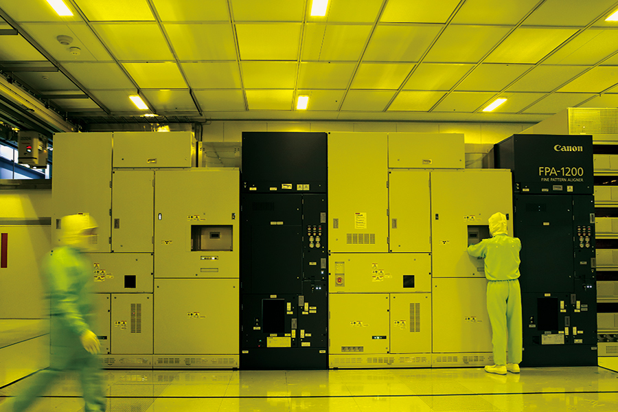
Semiconductor lithography equipment plays a vital role in production of semiconductor devices and is counted on continuous operation. Canon’s new remote services contribute to high productivity.
LEARN MORE

flexible
Making displays even thinner, more beautiful, and energy-saving. Canon leads the world in the manufacture of OLED displays, which enhance convenience and offer even greater possibilities.
LEARN MORE
Canon Tokki boasts an overwhelming share of the manufacturing equipment that produces OLED panels used in smartphones and televisions. It supports next-generation manufacturing in cooperation with other Canon Group companies.
LEARN MORE
At the Kioxia Yokkaichi Plant, trials are underway for semiconductor lithography equipment that utilizes Canon's "nanoimprint" technology, which can significantly reduce manufacturing costs.
LEARN MORE