
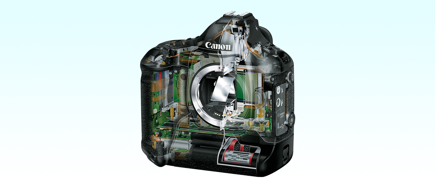
Professional photographers around the world place immense trust in Canon's digital SLR cameras. The company leads the imaging world with its innovative products, which realize high-quality images through such groundbreaking technologies as proprietary lenses, CMOS sensors and image processors.
2018/12/27Featured Technology
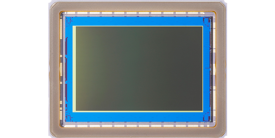
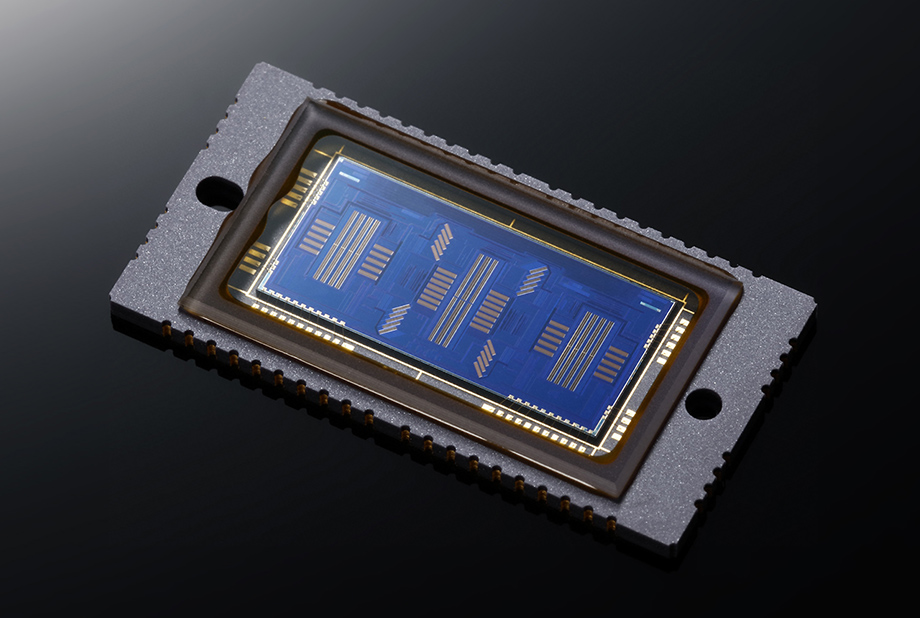
Building on proprietary technologies, Canon develops and manufactures CMOS in-house. Sensors are available in 35 mm full-frame and APS-C sizes.
Features of Canon's CMOS sensors include a large size and high resolution (a maximum of approximately 50.6 megapixels in the case of the 35 mm full-frame CMOS), exceptionally high sensitivity (minimal noise) and wide dynamic range. In addition, High-speed continuous shooting at a rate of approximately 14 frames per second*, 4K video recording, and other functions to achieve a range of expression for both still images and video.
#Imaging technologies#Electrical engineering#Semiconductors
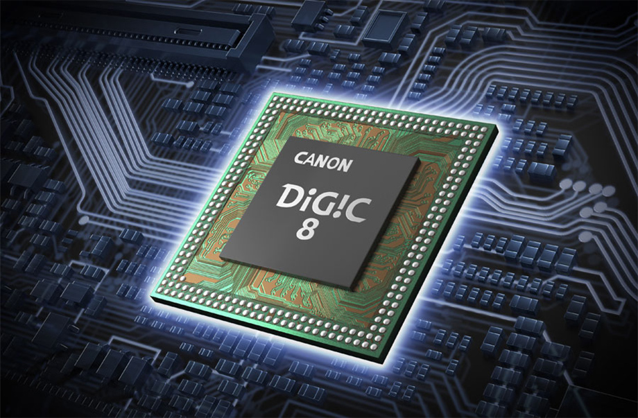
DIGIC 8
When light enters the camera via the lens, it is converted to an electrical signal by the image sensor. Canon's DIGIC image processor1 is then used to generate image data based on the signal. This data reproduces natural colors with rich gradations and little noise. DIGIC uses proprietary algorithms to perform processing optimized for still images and videos, which makes it possible to reduce noise while maintaining high resolution, even when shooting in low-light scenarios. Additionally, Canon's DIGIC image processor is a high-performance system LSI2 that uses a proprietary architecture to make high-speed processing possible, including the creation and processing of beautiful still images and videos, autofocus, image-stabilization evaluation operations, continuous shooting processing and Live View display.
#Imaging technologies#Automation#Mechanical engineering#Electrical engineering#Physics
Dual Pixel CMOS AF is revolutionary image-plane phase detection AF technology that uses a CMOS sensor with a new structure equipped in which all pixels can perform both imaging and phase detection AF functions.
With Dual Pixel CMOS AF sensors, each pixel consists of two separate photodiodes, allowing it to simultaneously output an imaging signal and signal that can be used for phase detection AF. Light can be gathered by these two photodiodes independently. Signals from each photodiode are detected when performing phase detection AF, and for imaging, the two photodiodes work in tandem to output an image signal as one pixel.
Dual Pixel CMOS AF Video (11 seconds)
*In order to view videos, it is necessary to consent to the use of cookies by our website. If the videos are not displayed, please click the "Cookie Settings" and accept cookies.
#Imaging technologies#Automation#Electrical engineering
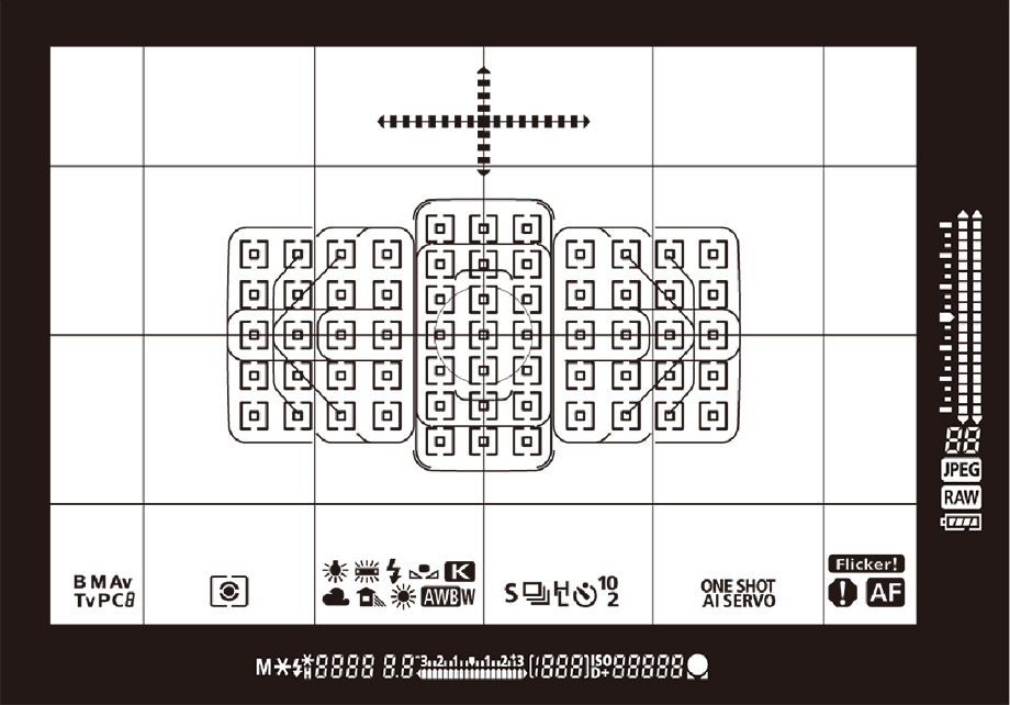
The autofocus (AF) technology of Canon's EOS-series SLR cameras debuted in 1987, making an impact with its speed and ease of use. Since that time, Canon has continued to develop and evolve AF technology into a digital camera legacy: from its initial AF with a single focus point at the center of the viewfinder to 3-point AF in 1990, 5-point AF in 1992, 45-point Area AF in 1998, and 61-point Area AF in 2012.
AF Sensor
This AF frame, which has a high-density arrangement of 61 points, has superior ranging capabilities, including the ability to handle an f/8 aperture at all focus points and an increased low-brightness limit at the central point.
Focus-Point FOV Layout Diagram
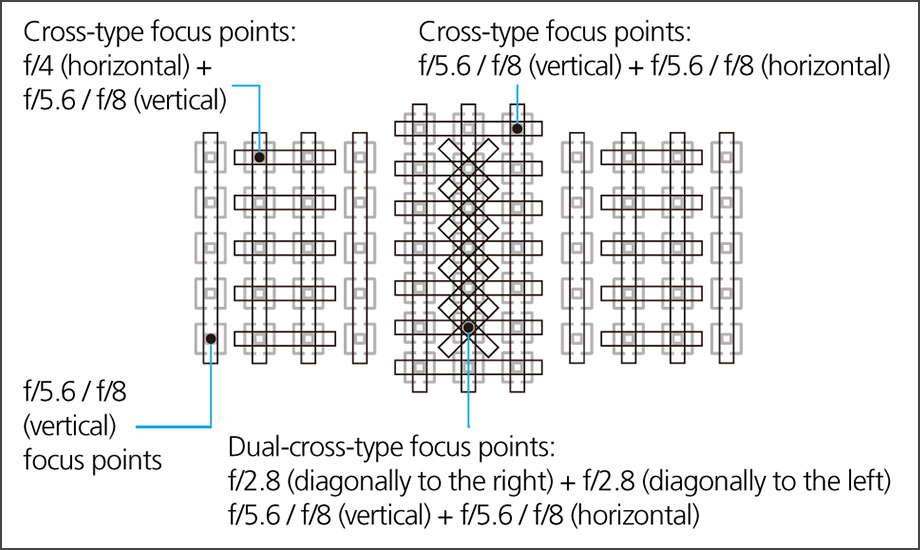
Focus-Point Pattern Conceptual Diagram