History
The history of Canon's intellectual properties in the industrial field
Industrial
-
1960sEntry into the semiconductor-related field
Canon's history of entering the industrial field began in the 1960s. Canon began developing lenses for semiconductor device manufacturing, which had a strong affinity with optics, one of Canon's core technologies, and completed the U100mm F2.8 high-resolution lens in 1967. Subsequently, we began to develop semiconductor lithography equipment. In 1970, Canon announced the PPC-1, a projection-type equal-magnification printing system with a U170mm projection lens, alignment microscope, and alignment mechanism, simultaneously in both Japan and the United States, which attracted a great deal of interest. This product was the first semiconductor lithography equipment made in Japan. Canon's intellectual property activities in the industrial equipment field also started in line with this development, and in 1969, the year before the announcement of the product, we filed a patent application for an equal magnification exposure machine.

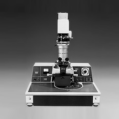
PPC-1, the first Japanese-made semiconductor lithography equipment -
1970sBirth of the stepper
In the 1970s, Canon began to develop an auto-alignment mechanism using lasers, and in 1976 we filed a patent application for a scanning-type light detecting device. This technology was incorporated into what was at that time the world's first laser-based auto-alignment mechanism in the PLA-500FA semiconductor lithography equipment, launched in 1978. After this product, the laser-based auto-alignment mechanism became the industry standard for semiconductor lithography equipment. It was also applied to the alignment technology of Canon's first stepper, the FPA-1500FA, which was announced at SEMICON Japan in 1983.

The PLA-500 series, which became a bestseller (Photo: PLA-501FA) 
FPA-1500FA, Canon's first stepper -
1980sDevelopment of FPD (Flat Panel Display) lithography systems
In 1980, Canon launched the MPA-500FA (1.5 µm resolution) catoptric projection type semiconductor lithography equipment using mirror optical system technology, which led to the current generation of FPD lithography systems. This model was equipped with technology related to a mirror optical system for which a patent application was filed in 1975. Later, an optical system from the same patent application filing was also used in Canon's first FPD lithography system, the MPA-1500, launched in 1986. In 1985, Canon filed a patent application for an invention related to synchronous scanning of masks and substrates, and this technology was incorporated into the MPA-5000 FPD lithography system released in 1997. In addition, it received the Minister of International Trade and Industry Award from the Japan Society for the Promotion of Machine Industry for its contribution to improving FPD productivity.

MPA-500FA, for 256K DRAM production using mirror optical system technology 
MPA-1500 FPD lithography system -
Early 1990sStepper development
In the early 1990s, Canon created inventions related to stage structures using air bearings and active dampers for suppressing vibrations transmitted to the projection optical system, and filed many patent applications. These technologies were incorporated in the FPA-3000i4, an i-line stepper for 64-megabit DRAM mass production launched in 1994. This machine was equipped with what was then the world's highest-level i-line lens, with a numerical aperture (NA) of 0.63 and resolution of 0.35 μm, and was newly equipped with an air bearing stage.

FPA-3000i4 i-line stepper for 64-megabit DRAM mass production -
Late 1990sFrom i-line to excimer laser
In response to semiconductor device die shrinks, excimer lasers were adopted as light sources in the late 1990s. In the early 1980s, Canon began filing patent applications for techniques for narrowing the band of excimer lasers and dose control technology, and was ahead of the times in advancing development and intellectual property activities. These technologies were incorporated in the FPA-3000EX3, a stepper that uses an excimer laser, which was launched in 1996.

The FPA-3000EX3, which uses a KrF excimer laser as its light source -
2000s and afterDevelopment of nanoimprint lithography
In 2004, Canon began research into nanoimprint technology targeting further semiconductor device die shrinks. In 2009, with the aim of mass-producing next-generation semiconductor lithography equipment using this technology, we began joint development with the U.S. company Molecular Imprinting, Inc., a world leader in the number of registered patents and technological capabilities in nanoimprinting technology, and other major semiconductor manufacturers. In 2014, we made Molecular Imprints, Inc. a wholly owned subsidiary (newly named Canon Nanotechnologies) and accelerated its development. The intellectual property division has been engaged in continuous intellectual property activities in collaboration with the development division since 2004, when research into nanoimprint technology began, up to the present day.
Intellectual Property History
by business field
-
Printing
The history of Canon's intellectual properties in the printing field
Read more
-
Medical
The history of Canon's intellectual properties in the medical field
Read more
-
Imaging
The history of Canon's intellectual properties in the imaging field
Read more
-
Industrial
The history of Canon's intellectual properties in the industrial field
Read more