Semiconductor Lithography Equipment
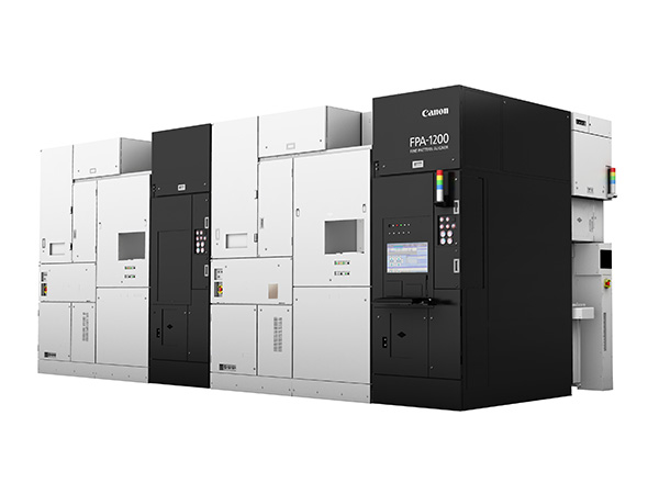
FPA-1200NZ2C
Nanoimprint lithography equipment
- Features
- Specifications
Basic Information
Model Name: FPA-1200NZ2C
Features
In contrast to conventional photolithography equipment, which transfers a circuit pattern by projecting it onto the resist coated wafer, the new product does it by pressing a mask imprinted with the circuit pattern on the resist on the wafer like a stamp. Because its circuit pattern transfer process does not go through an optical mechanism, fine circuit patterns on the mask can be faithfully reproduced on the wafer. Thus, complex two- or three-dimensional circuit patterns can be formed in a single imprint*1, which may reduce the cost of ownership (CoO).
Canon's NIL technology enables patterning with a minimum linewidth of 14 nm*2, equivalent to the 5-nm-node*3 required to produce most advanced logic semiconductors which are currently available. Furthermore, with further improvement of mask technology, NIL is expected to enable circuit patterning with a minimum linewidth of 10 nm, which corresponds to 2-nm-node.
The new product employs newly developed environment control technology that suppresses the contamination with fine particles in the equipment. This enables high-precision alignment which is necessary for the manufacture of semiconductors with an increasing number of layers and the reduction of defects due to fine particles, and enables the formation of fine and complex circuits, contributing to the manufacture of cutting-edge semiconductor devices.
Since the new product does not require a light source with a special wavelength for fine circuit, it can reduce power consumption significantly compared to the photolithography equipment for currently available most advanced logic semiconductors (5-nm-node with 15 nm linewidth), thereby contributing to CO2 reduction.
The new product can be used for a wide range of applications, such as metalenses*4 for XRs with microstructures of tens of nanometers, in addition to logic and other semiconductor devices.
- *1 A pattern forming process of nanoimprinting.
- *2 one billionth of a meter.
- *3 “nm-node”: a generation of semiconductor technology.
- *4 An element with the same function as a lens by controlling light with a fine structure smaller than the wavelength of visible light.
Specifications
| Field Size | 26 × 33 mm |
|---|---|
| Mask Size | 6 inch |
| Wafer Size | 300 mm (12 inch) |
| Overlay Accuracy | ≦ 4 nm |
| Main Body Dimensions | (W) 2700 × (D) 6600 × (H) 2830 mm (2station) |