News Release
January 13, 2026
Canon Inc.
Canon achieves world first with novel inkjet-based wafer planarization, delivering dramatically smoother wafer surfaces
TOKYO, January 13, 2026—Canon Inc. announced today that Canon has become the first in the world1 to develop and practically implement a groundbreaking wafer planarization technology called inkjet-based adaptive planarization (IAP) by leveraging its expertise in nanoimprint lithography. Canon aims to commercialize equipment incorporating IAP technology in 2027 for use in advanced semiconductor manufacturing, including the manufacture of logic and memory devices.
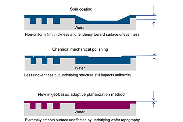
Planarization—the process of smoothing out surface irregularities on wafers—is an indispensable process in semiconductor manufacturing. As multiple layers of films and wiring are built up, even slight unevenness on wafer surfaces can cause critical dimension2 errors and pattern edge misalignment. These issues significantly impact productivity, especially as semiconductor devices become increasingly miniaturized and three-dimensional, driving demand for ultra-precise planarization technologies. Traditional planarization methods include spin coating, which is used to form thin films that create smooth upper surfaces, and chemical mechanical polishing, which involves repeated physical polishing of wafers. These approaches involve multiple steps, however, adding to the complexity and cost of the overall process.
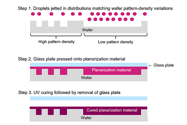
Canon developed a nanoimprint lithography method in which an inkjet system is used to apply resist onto wafers before a patterned mask is pressed onto the surface like a stamp to transfer circuit patterns. Canon then incorporated this technology into the FPA-1200NZ2C semiconductor manufacturing system, launched in October 2023. Building on this foundation, Canon developed IAP by adapting key elements of nanoimprint lithography for use in the planarization process.
An inkjet is used to dispense light-curable material onto areas of the wafer in a precisely tuned manner that matches surface topography, including the distribution of circuit patterns. High-precision planarization is achieved by then pressing a flat glass plate onto the wafer. This makes it possible to precisely level the entire surface of a 300 mm-diameter wafer in one stamping process, regardless of variations in the underlying circuit design or topographical density. Topographical irregularity is thereby reduced to 5 nm or less, facilitating the uniform layering of structures—essential for subsequent downstream processing.
Canon and Canon Nanotechnologies will be presenting their work on IAP at the upcoming SPIE Advanced Lithography and Patterning Conference scheduled on Wednesday, February 25th at the San Jose Convention Center. The presentation will include details on the IAP process and initial results.
- 1
According to Canon data (January 12, 2026).
- 2
Critical dimension: the specific circuit dimension regarded as critical for semiconductor device performance.