Creating Manufacturing Innovations for a Connected World - Canon Semiconductor Lithography Equipment
The most important step in semiconductor device fabrication is the lithography where a circuit pattern is transferred from a mask to a wafer or panel by precision Semiconductor Lithography Equipment commonly referred to as steppers or scanners.
Canon has developed a lineup of Semiconductor Lithography Equipment designed to meet the technical requirements of a wide range of applications in addition to traditional semiconductor wafer processing.
Please refer to this for information about Canon Group's semiconductor manufacturing process.
News
- Product lineup
- Related lineup
- Videos
Semiconductor Lithography Equipment Lineup
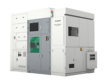
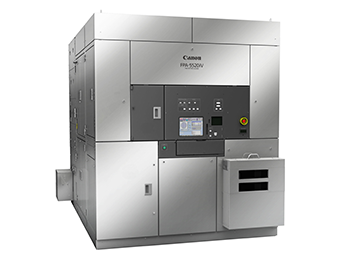
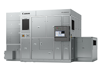
KrF Scanners / Steppers
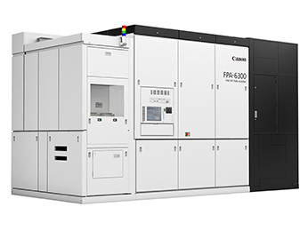
High Resolution / High Productivity KrF Scanner
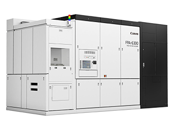
Wide-Field / High Productivity KrF Scanner
KrF Stepper for IoT devices
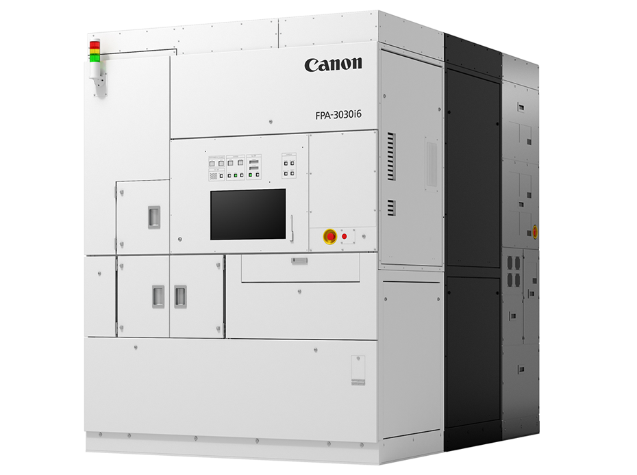
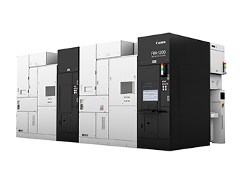
i-line Steppers for Front-End-Of-the-Line (FEOL) Applications
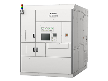
High Productivity / High Overlay Accuracy i-line Stepper
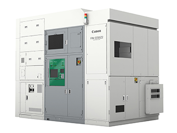
Wide-Field / High Resolution i-line Stepper
i-Line Stepper for smaller substrates of 200mm or less
i-Line Stepper supporting reduced Cost-of-Ownership manufacturing for small substrates
Low NA i-line stepper for power devices, IoT related devices, and smaller substrates of 200mm or less
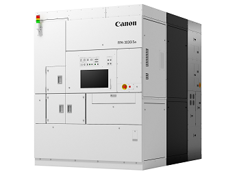
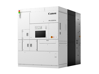
i-line Steppers for Back-End-Of-the-Line (BEOL) and Advanced Packaging Applications
HR Option / LF Option
i-line stepper for advanced packaging with an optional lineup supporting high resolution and large exposure field
i-line stepper compatible with large panels at 1.0 μm resolution
Nanoimprint Lithography
Nanoimprint lithography equipment
Related system for Semiconductor Manufacturing
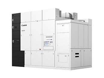
"MS-001" is a high-precision wafer alignment measurement device for semiconductor lithography systems.
Service for Semiconductor Lithography Equipment
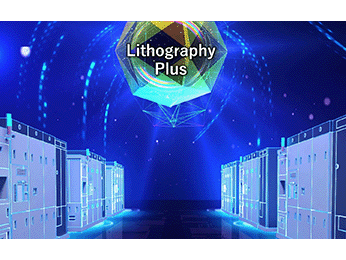
“Lithography Plus” is a solution platform offering Canon’s support know-how to help maximize productivity for semiconductor lithography systems.
Videos
*In order to view videos, it is necessary to consent to the use of cookies by our website. If the videos are not displayed, please click the "Cookie Settings" and accept cookies.