- Features
- Specifications
- Video
Basic Information
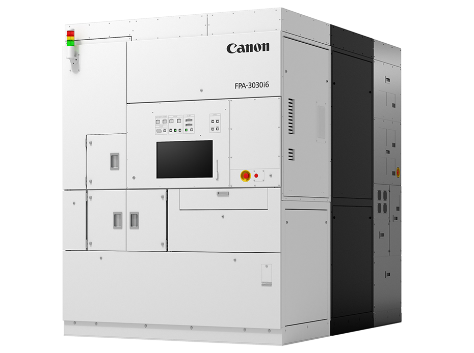
Model Name: FPA-3030i6
Features
The lens is made of high-transmittance glass material that reduces lens aberrations occurring during exposure by more than 50%1 when compared to previous stepper models2. Higher transmittance also helps reduce exposure time while maintaining pattern fidelity, even under high exposure dose conditions.
Improving lens transmittance will also increase exposure intensity and shorten the exposure time required for each process. The FPA-3030i6 standard productivity for 8 inch (200 mm) wafers has increased3 to 130 wafers per hour from 123 for the previous stepper models.
Additionally, since the lens is highly durable, lens transmittance decrease over time is reduced and productivity can be maintained over the life of the system.
The NA (numerical aperture) range has also been expanded from 0.45~0.63 in the previous model to 0.30~0.63. Allowing for a smaller NA enables customers to select the optimum NA for each device layer.
Optional products including a wafer handling system for special substrates are available for order to meet users' manufacturing needs for various emerging semiconductor devices including high-power and high-efficiency green devices.
The FPA-3030i6 is designed to support a wider range of device fabrication thanks to a variety of available process options for silicon (Si) as well as sapphire and compound semiconductor materials such as silicon carbide (SiC), gallium nitride (GaN) and gallium arsenide (GaAs) substrates.
Canon will offer wafer feeding options enabling handling of substrates from 2 inches (50 mm) to 8 inches (200 mm) in diameter, as well as thick, thin and warped substrate handling.
- 1 Under Canon's standard exposure conditions
- 2 FPA-3030i5a (released in March 2021)
- 3 8 inches (200 mm) wafer
Specifications
| Resolution | ≦ 0.35 µm |
|---|---|
| NA (Numerical Aperture) | 0.45~0.63(Variable) *Options Required 0.30~0.63 |
| Reduction Ratio | 1:5 |
| Field Size | 20mm x 20mm(5inch)/ 22mm x 22mm(6inch) |
| Exposure Wavelength | i-line 365 nm |
| Reticle Size | 5 inch / 6 inch (Selection) |
| Wafer Size | 50mm(2inch) / 75mm(3inch) / 100mm(4inch) / 150mm(6inch) / 200mm(8inch) (Selection) |
| Overlay Accuracy | ≦ 40 nm |
| Main Body Dimensions | (W) 1,900× (D) 2,600× (H) 2,450mm (Included exhaust duct: 2,650mm) |
| Major Options | High intensity option Low-NA option Wafer Handling Kit for Special Substrates PC Remote Console GEM-compliant online software Through Silicon Alignment |
Video
*In order to view videos, it is necessary to consent to the use of cookies by our website. If the videos are not displayed, please click the "Cookie Settings" and accept cookies.