Industrial

Ultra precision manufacturing equipment underpinning the digital economy
Canon supports global semiconductor and display production with super-precision technology.
Broad coverage of semiconductor production processes helps stabilize advanced chip supplies
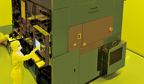
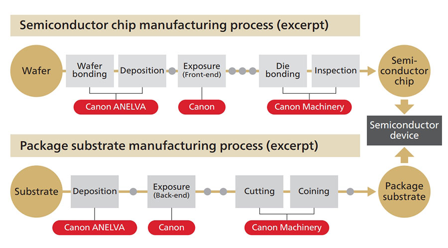
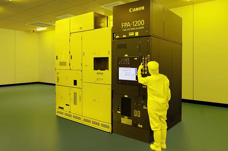
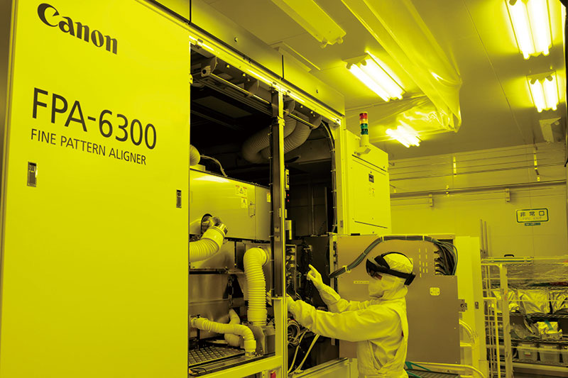
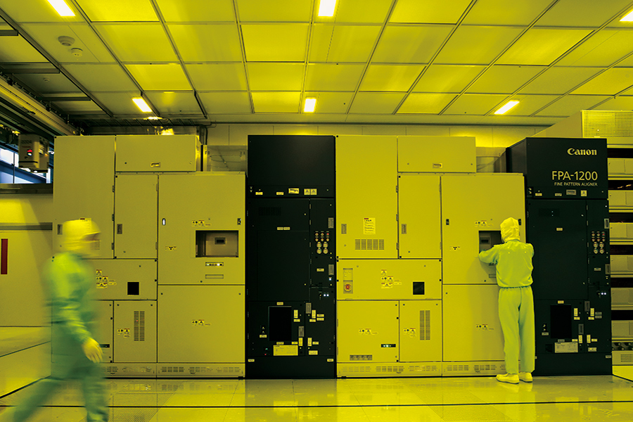
Semiconductor chips are used in various products. The Canon Group works together to provide a wide range of production equipment. Its lithography equipment forms circuit patterns, while Canon ANELVA’s sputtering equipment forms thin metal films. Canon’s lithography equipment has made a significant contribution to the development of semiconductors for AI applications, particularly in packaging processes that require the integration of multiple functions and precise alignment of fine layers. The company is also at the forefront of advanced lithography that stitches multiple exposure areas to form a single large package, while Canon Machinery’s die bonders securely mount chips on lead frames.

Super-precision technology behind the fine resolution of ever-larger high-quality displays
High-definition displays, including those in smartphones, PCs, and 4K and 8K TVs, are ubiquitous and essential in today’s digital society. Canon’s flat-panel display (FPD) lithography equipment, which transfers fine display circuit patterns onto large glass substrates, supports OLED and LCD display production with super-precision technology. Adoption of OLED displays is growing, due to their ability to reproduce deep blacks, as well as their thin, lightweight, and energy-efficient design. Canon Tokki, which realized mass production of OLED displays with world-leading vapor deposition equipment, is focused on developing technology for vapor deposition that works with new production equipment and new materials.

Nanoimprint lithography enables miniaturization while significantly reducing energy consumption for advanced semiconductor production
Semiconductor devices have continued to evolve, achieving higher performance through finer circuit geometries. Canon’s nanoimprint lithography (NIL) technology transfers superfine circuit patterns like a stamp, greatly reducing the power consumed by production processes to approximately one-tenth of conventional methods. It has also developed technology to suppress tiny-particle generation and contamination—a long-standing challenge—and is now pushing toward the cutting-edge 2-nm node.* NIL technology can be applied to wafer surface planarization—a critical process in advanced semiconductor production—providing strong backing for the manufacturing of advanced semiconductors.
- * Nodes are a naming convention for the generations of semiconductor production process technologies.

Society realized by Industrial Equipment Business
Canon's nanoimprint lithography can make the semiconductor manufacturing equipment much smaller and use much less energy thanks to its simple process.
Learn more
Semiconductor lithography equipment plays a vital role in production of semiconductor devices and is counted on continuous operation. Canon’s new remote services contribute to high productivity.
Learn more

flexible
Making displays even thinner, more beautiful, and energy-saving. Canon leads the world in the manufacture of OLED displays, which enhance convenience and offer even greater possibilities.
Learn more
Canon Tokki boasts an overwhelming share of the manufacturing equipment that produces OLED panels used in smartphones and televisions. It supports next-generation manufacturing in cooperation with other Canon Group companies.
Learn more
At the Kioxia Yokkaichi Plant, trials are underway for semiconductor lithography equipment that utilizes Canon's "nanoimprint" technology, which can significantly reduce manufacturing costs.
Learn more