Society realized by Industrial Equipment Business
As semiconductors evolve, semiconductor production is also moving forward
Nanoimprinting — a game-changer for semiconductor device production
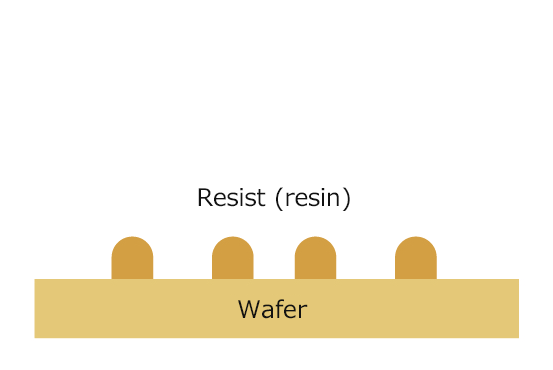
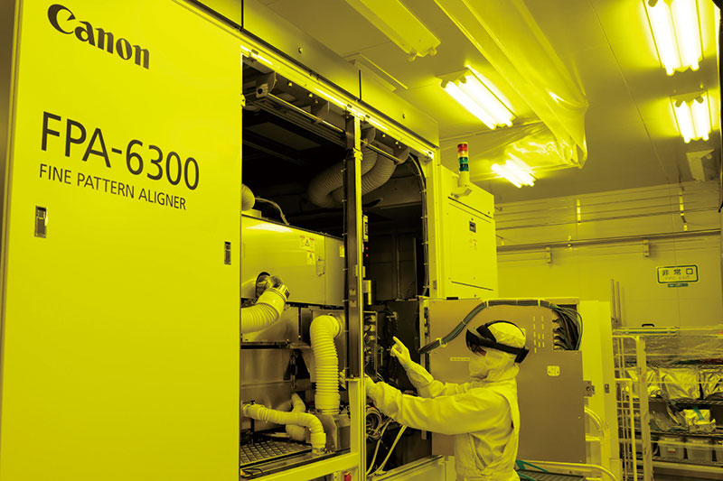
Semiconductor devices are vital for our modern convenience and lifestyles. The technologies that will transform society — such as autonomous driving, the metaverse, and generative AI — would not exist without advances in semiconductor devices. A crucial step in producing semiconductor devices, which involves forming repeated microscopic electrical circuits on a semiconductor wafer,*1 is transferring the circuit patterns onto a resin material, called the resist, that is applied to the wafer. Lithography, the most common technology today, uses light controlled by lenses to expose the circuit patterns onto the wafer. However, to create higher performing devices, circuit linewidths must be made finer, which requires larger light sources and enormous amounts of power.
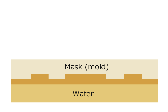
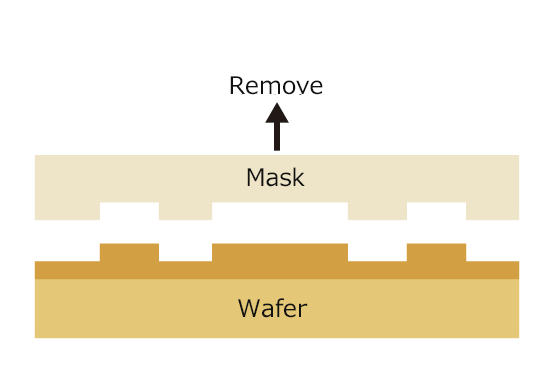
Canon's nanoimprint lithography (NIL) technology is expected to revolutionize current practices in semiconductor production. NIL is a simple process in which superfine patterns, called masks, are pressed into the resist, much like a stamp, to form circuits. This simplicity means the equipment can be much smaller and use much less energy.
- *1 Wafers are extremely thin semiconductor slices
Nanoimprint lithography process
NIL might be used to fabricate not only 3D nanostructures but also cutting-edge semiconductor devices
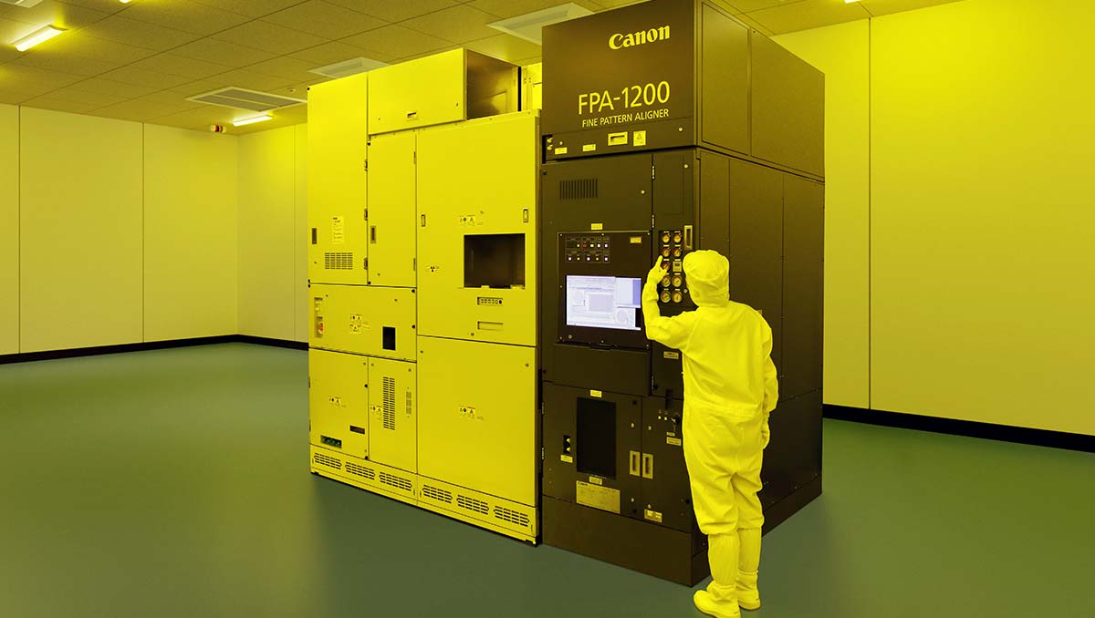
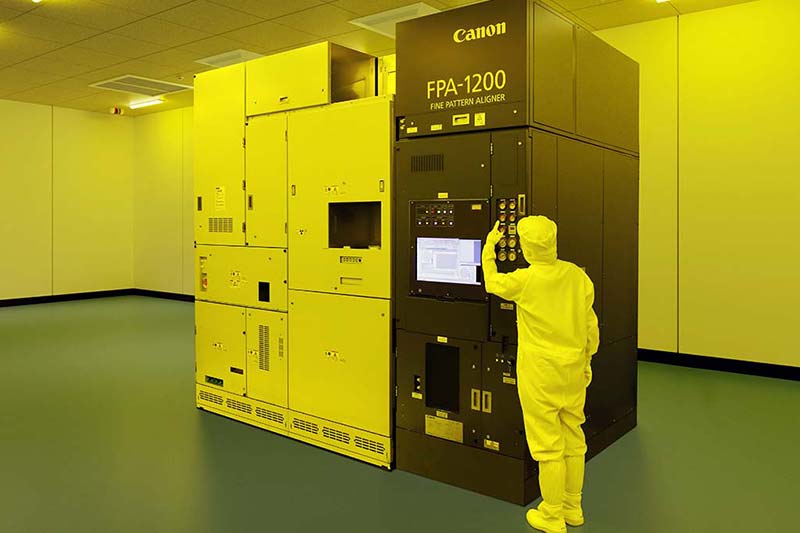
The most advanced semiconductor logic devices*2 today are produced with 5 nm node*3 technology. The node requires a minimum circuit linewidth of 14 nanometers. In the world of nanometers (nm), which represent a billionth of a meter, the main roadblocks are contamination by fine particles, overlay accuracy, and the technology to remove the mask from the resist. Canon has solved these issues with alignment and measurement technologies it developed for semiconductor production equipment and new technologies that inhibit fine-particle generation and contamination. In 2023, Canon finally launched a nanoimprint semiconductor manufacturing system that can mass produce 5 nm node devices with one-tenth the power of a conventional system. There are hopes that the technology will support the next-generation 2 nm node as well.
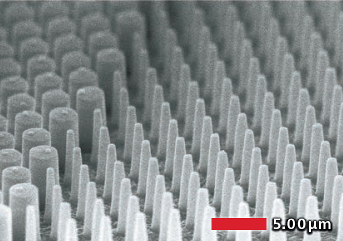
In addition to producing semiconductor devices, nanoimprinting is a low-cost technology for forming finely detailed, complex 3D structures. For example, flat lenses that control light with 3D structures having geometries smaller than the wavelength of visible light are no longer merely a dream but a reality. We can look forward to nanoimprinting-inspired breakthroughs in many industries.
- *2 Semiconductor devices, such as CPUs, that process data, perform controls, and carry out other functions as the brains of electronic devices
- *3 Nm nodes are how the generations of semiconductor manufacturing process technologies are named
Society realized by Industrial Equipment Business
Canon's nanoimprint lithography can make the semiconductor manufacturing equipment much smaller and use much less energy thanks to its simple process.
LEARN MORE
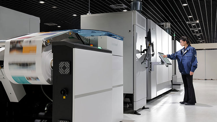
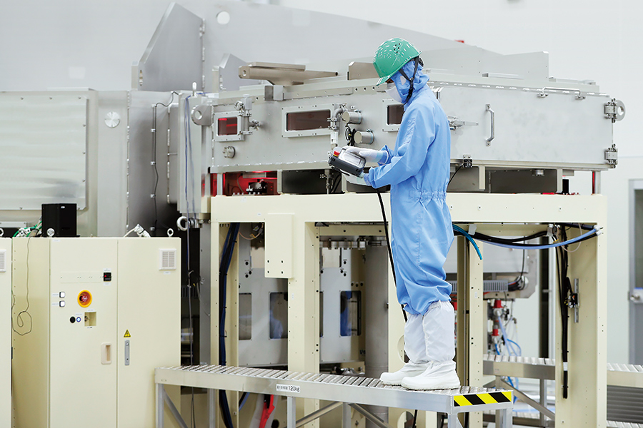
Semiconductor lithography equipment plays a vital role in production of semiconductor devices and is counted on continuous operation. Canon’s new remote services contribute to high productivity.
LEARN MORE

flexible
Making displays even thinner, more beautiful, and energy-saving. Canon leads the world in the manufacture of OLED displays, which enhance convenience and offer even greater possibilities.
LEARN MORE
Canon Tokki boasts an overwhelming share of the manufacturing equipment that produces OLED panels used in smartphones and televisions. It supports next-generation manufacturing in cooperation with other Canon Group companies.
LEARN MORE
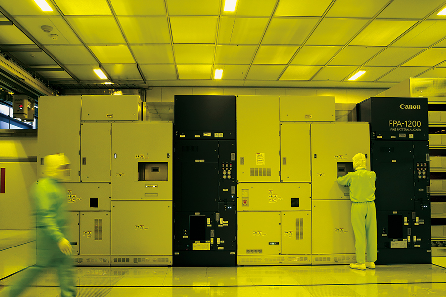
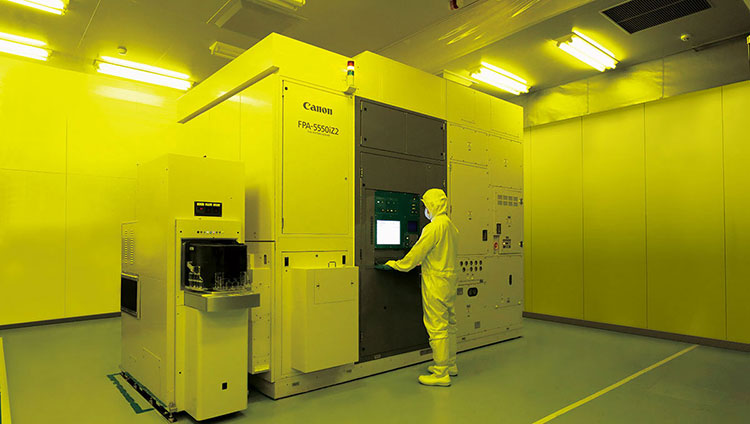
At the Kioxia Yokkaichi Plant, trials are underway for semiconductor lithography equipment that utilizes Canon's "nanoimprint" technology, which can significantly reduce manufacturing costs.
LEARN MORE