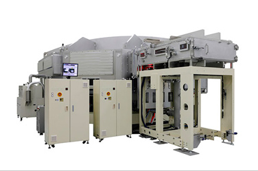
Technology in ProductsSemiconductor Lithography Equipment
Producing semiconductors indispensable for our daily lives
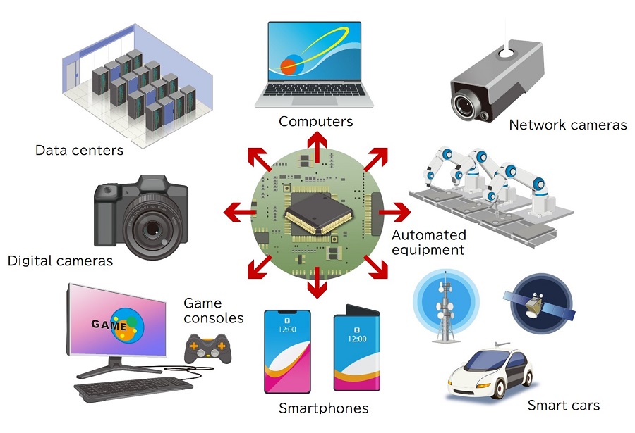
Automobiles, smartphones, home appliances, and other devices that are indispensable for our daily lives contain many semiconductors.Demand for semiconductors, particularly those used for generative AI and automated driving, is rapidly increasing. Semiconductor lithography equipment, which is essential for semiconductor production, requires the world's most advanced optical and control technologies.
January 23, 2025
Overview of Semiconductor Lithography Equipment
What is a semiconductor?
Semiconductors are substances such as silicon that have properties intermediate between conductors, such as metals, which conduct electricity well, and insulators, such as rubber and plastic, which conduct little electricity.
"Semiconductors" collectively refer to transistors1 and integrated circuits2 that use semiconductors as materials.
Read More
Canon’s semiconductor lithography equipment
Design, Manufacture, and Control Technologies Used in Projection Lenses with Higher Resolutions
Extraordinary Aberration Control for Achieving Theoretical Resolution Limits
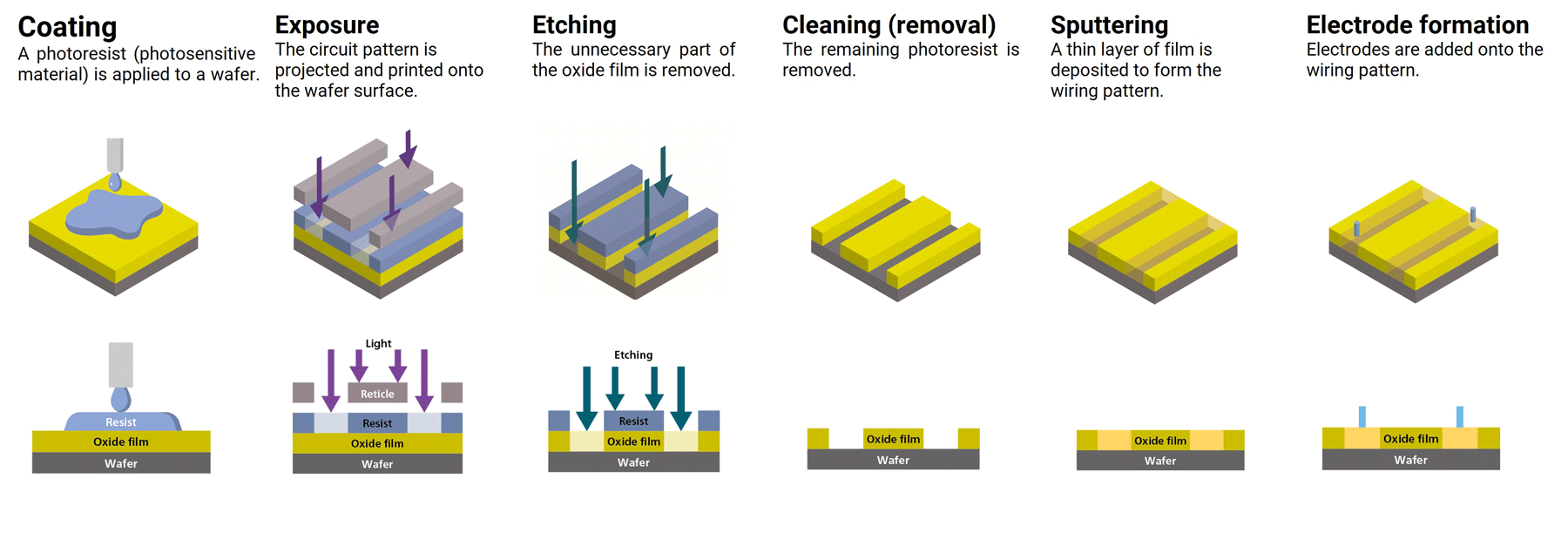
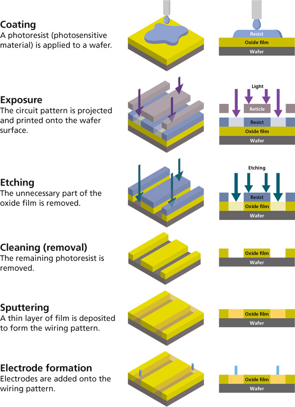
The circuit pattern drawn on the reticle is reduced by a projection lens and exposed onto the wafer.
The greater the resolution of the projection lens, the more delicate the patterns can be, increasing the circuit density.
Projection lens are manufactured using Canon's advanced optical design, assembly, and adjustment technologies, as well as lens polishing technology with a precision of several nanometers, both developed through the manufacture of cameras.
In addition, the resolution is enhanced by a mechanism in which the lens driver compensates for aberrations caused by slight environmental changes such as atmospheric pressure and temperature.
Semiconductor lithography equipment continues to operate 24 hours a day, 365 days a year. Over time, the circuit pattern passing through the lens becomes blurred or distorted due to heat during exposure and aging.
Canon developed projection lens that reduces distortion in projected circuit patterns by reviewing lens materials. The equipment can transfer accurate circuit patterns down to nanometers and can produce high-quality semiconductor chips.
Using Big Data Analysis Technology to Support Stable Operation
A support system to keep the equipment running is essential.
The semiconductor lithography equipment business is not completed when products are delivered to customers' factories.
It is important to have the customer-supporting technology to constantly maximize the performance of the equipment while it operates 24 hours a day, 365 days a year in the factory, to ensure customers' high productivity and exposure accuracy.
To this end, Canon developed a platform system that leverages its know-how in supporting equipment operation and the vast amount of data on semiconductor manufacturing processes, including the exposure process.
It supports stable operation of the equipment by automatically detecting abnormalities and restoring them by making full use of analysis technology for the enormous data accumulated.
Access here for details about Lithography Plus, Canon’s solution platform.


