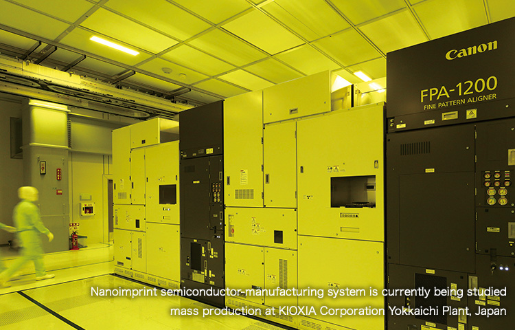
An Innovator Drastically Changing Convention in the Semiconductor Industry
Nanoimprint Lithography
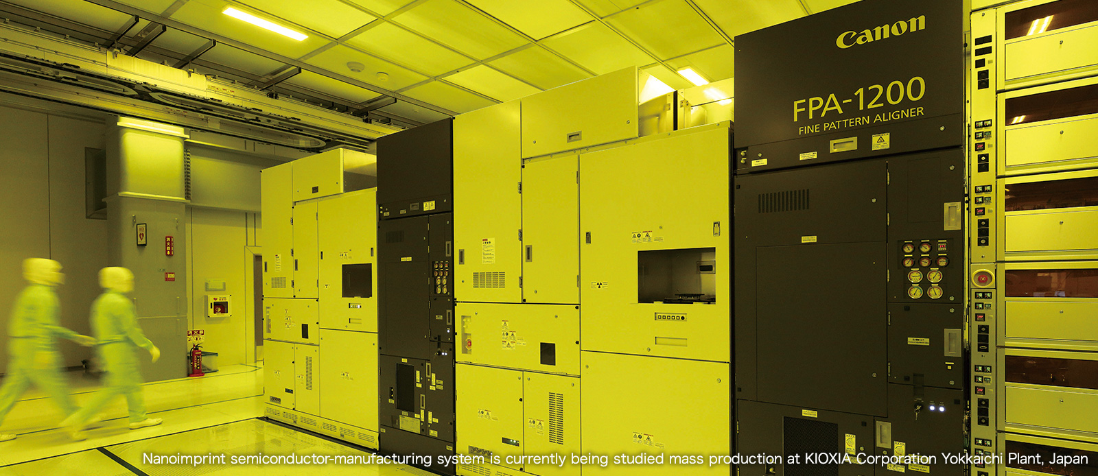
Technology fields responsible for the manufacture of semiconductor chips over half a century are about to be joined by an innovative technology. Canon is leading the world in working toward the mass implementation of nanoimprint lithography, utilizing technologies that it has developed through its semiconductor lithography equipment business, including a wafer stage that moves wafers accurately and at high speed, as well as high-precision alignment.
October 16, 2023
New Technology That Achieves Miniaturization with Low Power Consumption and at Low Cost
The evolution of semiconductor chips relates directly to the history of circuit miniaturization. The key to this miniaturization has been the shortening of light-source wavelengths and advances in lithography technologies that support miniaturization. In the early 1990s, 350nm patterns (nm: nanometer = one-billionth of a meter) were realized with i-line lithography systems. That miniaturization has since continued, with KrF/ArF lithography systems, and, in recent years, with EUV lithography systems.
Advances in lithography technology have contributed significantly to miniaturization and cost reduction of semiconductor chips. However, it has become increasingly difficult to achieve further miniaturization and manufacture complex semiconductor chips at low cost only through extensions of current technology.
Canon has achieved miniaturization at lower power consumption and lower cost with nanoimprint lithography (NIL), a new technology that is an alternative to conventional lithography technology. By enabling inexpensive production of patterns of 15nm or smaller, NIL is poised to revolutionize the semiconductor industry.
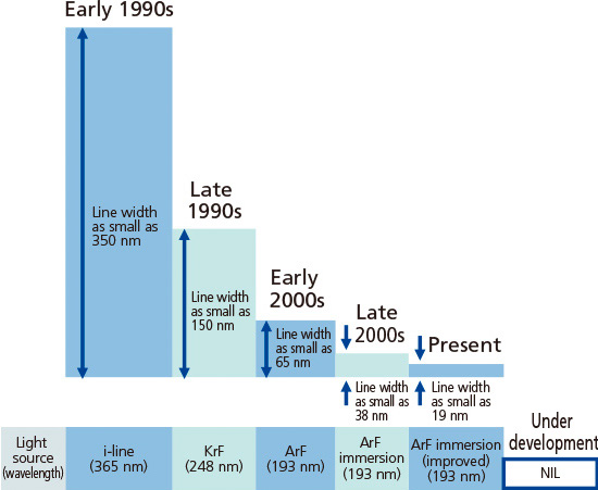
History of the miniaturization of circuit patterns
Confronting the Frequent Issues That Arise from a Simple Principle
Unlike conventional lithography technology that uses light to expose circuit patterns, NIL does not require a light source. Circuits are formed using a simple principle that involves transferring a circuit pattern mask (mold) onto the coated resist (resin) on the surface of the wafer (a thin silicone plate).
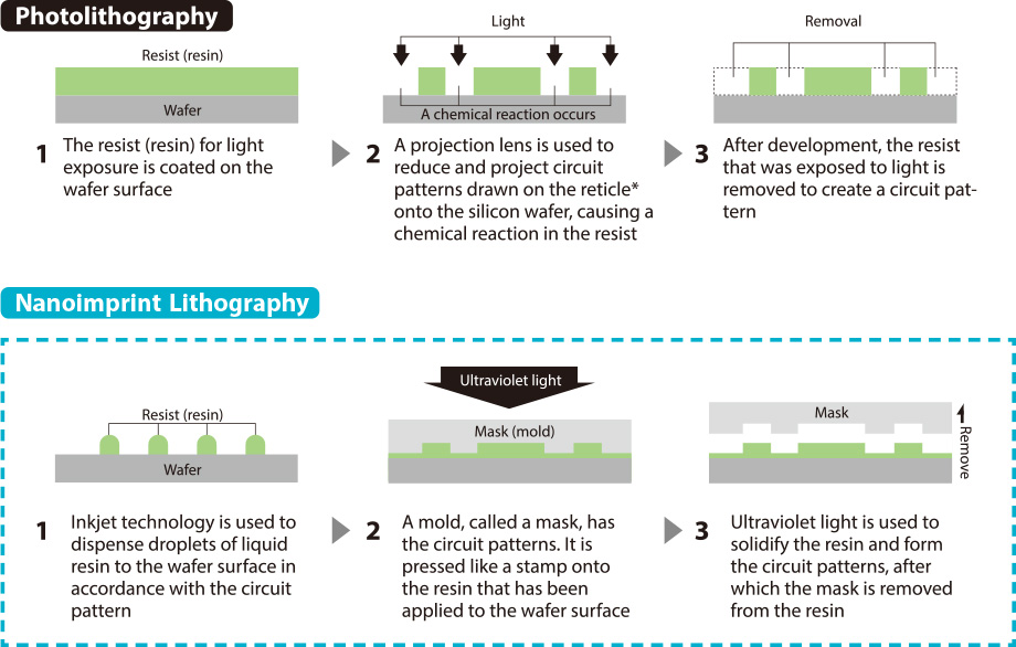
*Photomask used in semiconductor manufacturing
However, because of the system’s simplicity, there are numerous issues, and for a long time it has been said that practical application would be a challenge. To overcome a number of these issues, Canon began by working on technology to control the amount and positioning of the resin applied to the wafer surface. This technology precisely controls how much and where the resin is applied to prevent it from being squeezed out when the mask is pressed into the resin, while also ensuring the formation of a resin layer with a uniform thickness, regardless of the size or number of indentations on the mask being used.
Next, Canon developed a nanometer-level control technology to prevent the deformation of the convex circuit patterns formed in the resin, making it possible to cleanly remove the mask from the wafer.
Nanometer-level Alignment Technology
Because semiconductor chips are manufactured by stacking multiple pattern layers, it is necessary to achieve highly accurate alignment with patterns on lower layers. For NIL equipment, it is necessary to align transferred patterns that are tens of nm (nm: nanometer = one billionth of a meter) in size with nanometer-level accuracy. To achieve high-accuracy measurement of positional deviations, Canon has developed a system that makes it possible to measure positional deviations between the mask and the wafer in real time (Fig. 1). By using optimal moiré patterns as well as proprietary optical technologies and control technologies developed in collaboration with U.S.-based Canon Nanotechnologies, Inc. (CNT), NIL equipment can measure and correct for positional deviations between the mask and the wafer with nanometer-level accuracy.
In addition to the technology enabling high-accuracy measurement of positional-deviation information, matching technology enabling alignment with lower-layer patterns is also important. Canon has developed a proprietary matching system that achieves alignment by using laser irradiation to thermally deform the wafer (Fig. 2). This system makes it possible to change the heat input pattern and freely deform the wafer by controlling an ultra-fine mirror group called a Digital Micromirror Device (DMD). Instead of assuming that thermal deformation of the wafer worsens alignment precision as is conventionally thought, Canon has applied an innovative new approach to the alignment (Fig. 3).
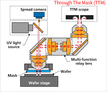
Fig. 1: TTM scope enabling the measurement of the positional deviations between the mask and wafer in real time
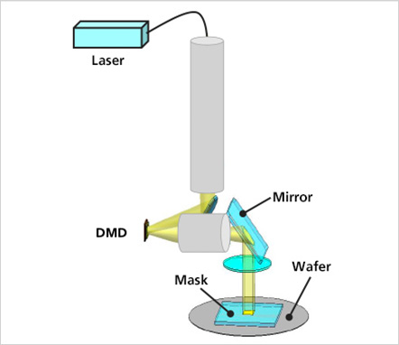
Fig. 2: Proprietary matching system
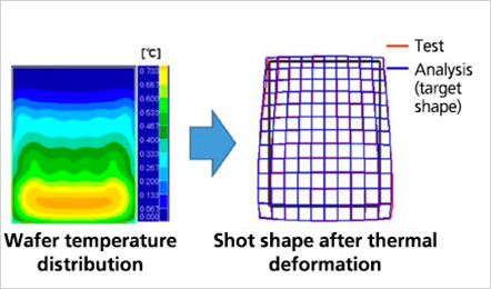
Fig. 3: Wafer temperature and shape after deformation
Nanoimprint Lithography (3 minutes 39 seconds)
*In order to view videos, it is necessary to consent to the use of cookies by our website. If the videos are not displayed, please click the "Cookie Settings" and accept cookies.
Particle Control Technology
“Particles” refers to particulate foreign matter. In the semiconductor industry, particles are a cause of defective devices, and have long been considered a problem. For NIL, because the mask is pressed against resist on the wafer to form patterns, particle management is extremely important. If particles end up between the mask and the wafer when pressing them together, it can cause not only defective devices but destruction of the pattern on the mask itself.
Starting at the earliest stages, Canon considered the eradication of particles an extremely high-priority issue. To address this, Canon spent a long time studying the use of ultra-high-performance filters in order to eliminate particles and utilizing design technology enabling the smooth flow of air into NIL equipment despite its complexity and many moving parts (Fig. 4). Canon also employs particle-elimination units to deal with particles that manage to get into the equipment, and has developed technology including air curtains (Fig. 5) that are used to section off ultra-clean environments for the most important areas by dividing areas based on how clean they are.

Fig. 4. Ultra-high-performance filter
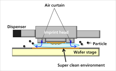
Fig. 5. Air curtain
Energy-saving Processing Technology and Expanding Applicable Devices
Recently, NIL’s energy-saving processing technology has also attracted attention. With existing lithography systems, complex circuit patterns are formed through repeated etching, but the overall manufacturing process is time-consuming and costly as a result. NIL, on the other hand, is able to form complex two- and three-dimensional patterns in a single pass, power consumption can be reduced by about one-tenth compared to advanced logic exposure technology.
Patterning performance

Two- and three-dimensional circuit patterns formed by NIL
Source: KIOXIA Corporation
Efforts by Canon, Dai Nippon Printing Co., Ltd., and KIOXIA Corporation in NIL received an Award of Excellence at the 49th Environmental Awards held in 2022, sponsored by the National Institute for Environmental Studies, Japan and the Nikkan Kogyo Shimbun, Ltd. and supported by the Ministry of the Environment. These three companies were recognized with their contribution for reducing power consumption during semiconductor manufacturing and for the technology which will support the rapid expansion of an IoT society.
In addition, the range of possibilities for semiconductors that can be manufactured using NIL is expanding to include DRAM which is memory for storing data, logic for processing data and controlling equipment, and even micro-optical elements in addition to semiconductors.


