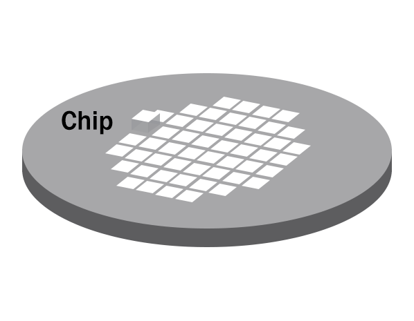
5,000 lines, yet as thin as a human hair!
Imprinting: the future of semiconductor lithography
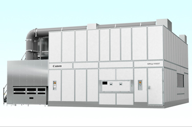
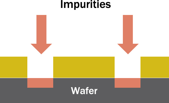
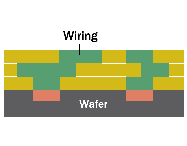
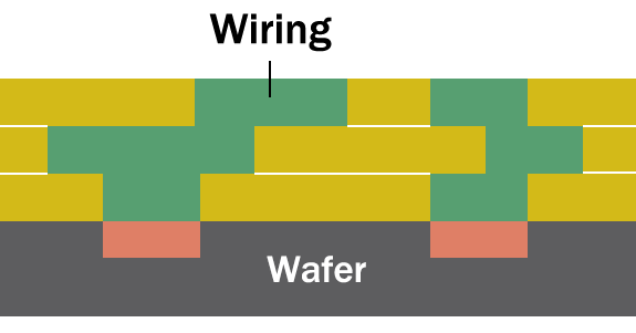
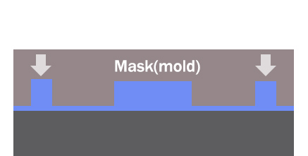
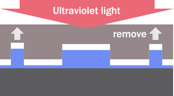
Next-generation semiconductor microfabrication technologyThe Story Behind Nanoimprint Lithography


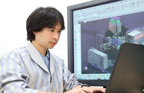


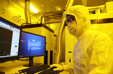
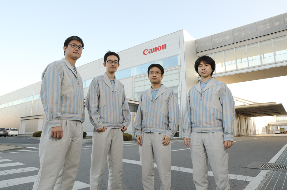
 Meeting with the Canon Nanotechnologies staff
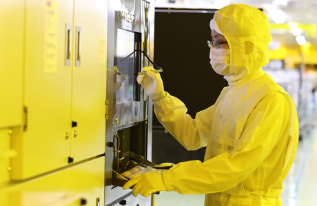
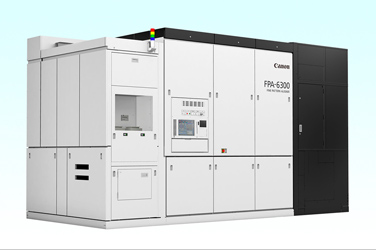
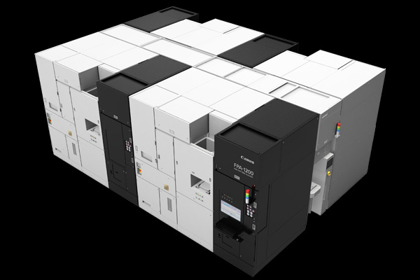
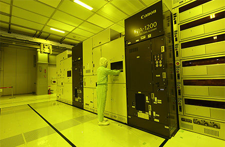 Fine-tuning of the nanoimprinting lithography equipment “FPA-1200NZ2C” in progress at Toshiba Memory's Yokkaichi Plant.