FPA-3030iWa
Low NA i-line stepper for power devices, IoT related devices, and smaller substrates of 200mm or less
- Features
- Specifications
- Video
Basic Information
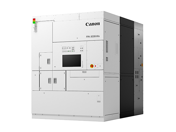
Model Name: FPA-3030iWa
Features
The FPA-3030iWa supports smaller substrates which are 200 mm or less in diameter.
- *A wide range of wafer sizes from 50mm (2inch) to 200mm (8inch) are supported.
- *FPA-3030 platform that has already demonstrated high reliability among customers in the market since release.
- *Wide exposure field of 52mm x 52mm is available.
Supports a wide range of needs for manufacturing of various devices and their processes
A 52 mm x 52 mm wide-field projection lens with a variable numerical aperture (NA) ranging from 0.16 to 0.24 delivers a large depth of focus (DOF) and enabling both high-precision exposure and creation of line width patterns with high uniformity.
Supports a variety of different wafer sizes and materials
The FPA-3030iWa can be equipped with a handling system that enables the selection of wafer diameters from 50mm (2inch) to 200mm (8inch) to support a variety of different compound semiconductor wafer sizes and materials.
Adopts an off-axis alignment scope with enhanced robustness
The FPA-3030iWa employs an off-axis alignment scope that measures wafer alignment marks through an optical path that does not pass through the projection lens. This allows the off-axis alignment system to use a wide range of alignment illumination wavelengths, providing robust alignment process optimization.
Improved throughput through newly redesigned hardware and software
The system updates make the FPA-3030iWa compatible with new options including wafer transfer functions supporting warped and transparent wafer processes such as silicon carbide and alignment system options that allow simultaneous X & Y alignment mark measurement to increase stepper productivity.
Specifications
| Resolution | ≦ 0.8 µm |
|---|---|
| NA (Numerical Aperture) | 0.24-0.16 (Variable) |
| Reduction Ratio | 1:2 |
| Field Size | 52mm x 52mm |
| Exposure Wavelength | i-Line 365nm |
| Reticle Size | 6inch |
| Wafer Size | 50mm(2inch) / 75mm(3inch) / 100mm(4inch) / 150mm(6inch) / 200mm(8inch) (Selection) |
| Overlay Accuracy | ≦ 100nm |
| Main Body Dimensions | (W) 1,900× (D) 2,600× (H) 2,450mm |
| Major Options | Wafer handling Kit for Special Substrates PC Remote Console GEM-compliant online software Pellicle particle Checker |
Video
*In order to view videos, it is necessary to consent to the use of cookies by our website. If the videos are not displayed, please click the "Cookie Settings" and accept cookies.