News Release
Canon commences sales of FPA-3030iWa i-line stepper for small substrates under 200 mm, supporting manufacturing of various devices
TOKYO, December 10, 2019—Canon Inc. announced today that the company has commenced sales of the FPA-3030iWa i-line semiconductor lithography system, or stepper*. The FPA-3030iWa supports small substrates under 200 mm in diameter that are commonly used for fabricating devices related to 5G communication and the Internet-of-Things (IoT), such as MEMS and sensors. The growth of power electronics applications in electric vehicles is also increasing demand for these wafers.
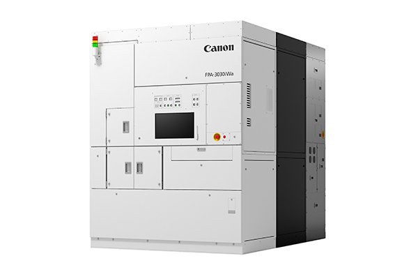
FPA-3030iWa
Through the combination of an overhauled lens design and a handling system that is compatible with a variety of different wafers, the FPA-3030iWa supports not only silicon wafer processing but also wafers used for the production of compound semiconductors. With increased exposure precision and support for various wafer types, this equipment meets a wide range of needs for innovative device manufacturing processes.
The FPA-3030iWa features a 52 mm x 52 mm wide-field projection lens with a variable numerical aperture (NA) ranging from 0.16 to 0.24 to deliver a large depth of focus (DOF) and make possible high-precision exposure and uniform line width resolution. Additionally, the FPA-3030iWa can be equipped with a handling system that enables the selection of wafer diameters from two inches (50 mm) to eight inches (200 mm) to support a variety of different compound semiconductor wafer sizes and materials.
FPA-3030iWa steppers also employ an off-axis alignment scope that measures wafer alignment marks through an optical path that does not pass through the projection lens. This allows the off-axis alignment system to use a wide range of alignment illumination wavelengths, providing robust alignment process optimization.
FPA-3030iWa steppers feature overhauled hardware and software evolved from the predecessor model FPA-3000iW (released in February 1995). The system updates make the FPA-3030iWa compatible with new options including wafer transfer functions supporting warped and transparent wafer processes such as silicon carbide and alignment system options that allow simultaneous X & Y alignment mark measurement to increase stepper productivity.
FPA-3030iWa precision imaging, wafer flexibility and alignment system are among the many features that combine to make the system applicable for a variety of device manufacturing processes.
- *i-line Stepper: A semiconductor lithography system that utilizes a 365 nm wavelength mercury lamp as the light source. 1 nm (nanometer) is 1 billionth of a meter.