FPA-8000iW
i-line stepper compatible with large panels at 1.0 μm resolution
- Features
- Specifications
- Video
Basic Information
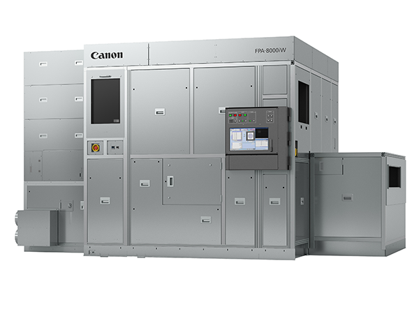
Model Name: FPA-8000iW
Features
i-line stepper "FPA-8000iW" for large panel substrates up to 515 x 510mm
- * Wide exposure field (52 mm x 68 mm or 55 mm x 65 mm).
- * High resolution of 1.0 μm is available across the wide exposure field.
- * High resolution and wide exposure field combine to provide high-productivity and further miniaturization, a larger device size and cost reduction for semiconductor packaging.
Supports high-productivity packaging on large substrates
In response to packaging processes that use panel substrates, Canon developed a new stepper platform capable of handling large 515 x 510 mm panel substrates. Severe warpage is also common in large panel substrates and the new platform and panel-feeding system can overcome up to 10 mm of panel warpage. As a result, the FPA-8000iW can help customers realize high-productivity and efficiency for PLP production of large packages.
Achieves a resolution of 1.0 μm that enables advanced packaging
Canon's original projection optical system supports a wide 52 x 68 mm exposure field while achieving 1.0 μm resolution, which is the finest resolution among packaging exposure systems that support panel substrate processes. As a result, advanced packaging technology such as Panel Level Packaging can innovate to provide high integration and flexibility in electronic system design.
Specifications
| Resolution | ≦ 1.0 µm |
|---|---|
| NA (Numerical Aperture) | 0.24-0.12 (Variable) |
| Reduction Ratio | 1:2 |
| Field Size | 52 mm x 68 mm or 55 mm x 65 mm |
| Exposure Wavelength | i-line 365 nm |
| Reticle Size | 6inch |
| Substrate Size | De facto size 515 x 510 mm can be processed (Max: 515 x 515 mm) |
| Overlay Accuracy | ≦ 200 nm |
| Main Body Dimensions | (W) 3,000 × (D) 4,800 × (H) 2,700 mm |
| Major Options | PC Remote Console Warped panel handling option (Vacuum Assist Unit) Resist Outgas Exhaust unit Pellicle Particle Checker |
Video
*In order to view videos, it is necessary to consent to the use of cookies by our website. If the videos are not displayed, please click the "Cookie Settings" and accept cookies.