- Features
- Specifications
- Video
Basic Information
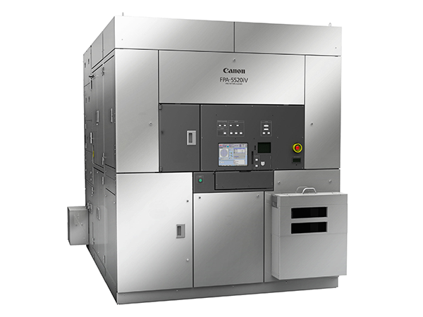
Model Name: FPA-5520iV / HR Option / LF Option / LF2 Option
Features
FPA-5520iV addresses next-generation packaging production challenges including Fan Out Wafer Level Packaging [FOWLP]
FPA-5520iV steppers have functions designed for processing of reconstituted FOWLP Wafers that consist of individual die that are mounted and encapsulated onto a carrier substrate for further processing. FOWLP wafers can suffer from severe warpage and die shift that must be overcome.
- *FPA-5520iV steppers employ a wafer handling system with flexible vacuum pads on robot end-effectors and other countermeasures to vacuum chuck warped substrates.
- *FPA-5520iV stepper wafer stages adopt a new wafer chucking system with increased suction to secure and flatten substrates, allowing high optical performance.
- *FPA-5520iV steppers utilize a new wide-field alignment scope with a field-of-view that is doubled vs. FPA-5510iV steppers, making automatic wafer alignment possible when wafers contain large amounts of die shift, to improve equipment utilization and productivity.
FPA-5520iV is a high performance i-line stepper
FPA-5520iV steppers achieve the highest levels of productivity among leading edge i-line steppers.*
FPA-5520iV steppers employ newly developed high-intensity illumination optics system that realizes an approximately 30% improvement in illumination intensity vs. FPA-5510iV steppers. FPA-5520iV steppers reduce exposure times for the thick photo-resist processes to boost back-end wafer processing capacity as much as **20%.
- *Among same-class i-line steppers. As of July 4, 2016 (Examination by Canon)
- **Throughput compared with the FPA-5510iV. 300 mm wafers, 60 shots, 10000J/m2 dose
FPA-5520iV inherits the benefits proven by the FPA-5510iV stepper
FPA-5520iV steppers inherit the proven high-resolution projection lens and imaging performance of the FPA-5510iV stepper.
FPA-5520iV steppers provide the same alignment system options as FPA-5510iV steppers to deliver robust and accurate overlay performance.
FPA-5520iV steppers adopt FPA-5510iV stepper console software with common operation procedures and easy recipe conversion.
FPA-5520iV HR Option achieves resolution of 0.8µm to support the advanced packaging process
In response to the growing demand for high-density redistribution layer wiring in the FOWLP market, "FPA-5520iV HR option" has been released since December 2018. The FPA-5520iV HR Option employs a new projection optical system that achieves a resolution of 0.8µm, the finest resolution available in packaging-oriented lithography systems.
- * Among same-class i-line steppers. With flatess equal to Si wafer. As of December 10, 2018. Based on a Canon survey.
FPA-5520iV LF Option realizes a single exposure with large field of 52×68mm
Equipped with a new projection optical system, a single exposure with large field of 52×68mm, which is more than 4 times the standard exposure field (26×33mm) of the lithography system in front-end process. This makes it possible to support heterogeneous integration where multiple large semiconductor chips are bonded.
FPA-5520iV LF2 Option contributes to 3D advanced packaging technologies with exposure fields of up to 100×100mm
The new FPA-5520iV LF2 Option features a fine 0.8µm resolution and 4-shot exposure with minimal distortion to make possible a wide 100×100mm exposure field. This in turn enables mass production of large and dense packaging with fine circuit patterns that integrate 2.5D and 3D technology.
View the news release (announcement for the press) for HR option
View the news release (announcement for the press) for LF option
View the news release (announcement for the press) for LF2 option
Specifications
| Resolution | FPA-5520iV: ≦1.5µm FPA-5520iV HR Option: ≦0.8µm FPA-5520iV LF Option: ≦1.5µm(High resolution option: ≦1.0µm) FPA-5520iV LF2 Option: ≦0.8µm |
|---|---|
| NA (Numerical Aperture) | FPA-5520iV:0.18~0.15 (Variable) FPA-5520iV HR Option:0.24~0.15 (Variable) FPA-5520iV LF Option:0.24~0.15 (Variable) FPA-5520iV LF2 Option:0.24~0.12 (Variable) |
| Reduction Ratio | 1:2 |
| Field Size | FPA-5520iV:52 mm x 34 mm FPA-5520iV HR Option:52 mm x 34 mm FPA-5520iV LF Option:52 mm x 68 mm FPA-5520iV LF2 Option:52 mm x 68 mm |
| Exposure Wavelength | i-Line 365nm |
| Reticle Size | 6 inch |
| Wafer Size | 300 mm (12 inch) |
| Overlay Accuracy | FPA-5520iV:≦0.15 µm FPA-5520iV HR Option:≦0.15 µm FPA-5520iV LF Option:≦0.15 µm FPA-5520iV LF2 Option:≦0.10 µm |
| Main Body Dimensions | (W) 2,300 x (D) 3,340 x (H) 2,700 mm |
| Major Options | Through-Silicon Alignment Scope (TSA-Scope) Wafer Edge Shielding Unit Wafer Edge Exposure Unit Chemical Filter Resist Outgas Exhaust Unit PC Remote Console GEM-compliant online software Pellicle Particle Checker EFEM Illumination System Purge Unit |
Video
*In order to view videos, it is necessary to consent to the use of cookies by our website. If the videos are not displayed, please click the "Cookie Settings" and accept cookies.