News Release
New Canon FPA-5520iV HR option for back-end i-line steppers achieves resolution of 0.8 µm to support the latest packaging trends
TOKYO, December 10, 2018—Canon Inc. announced today that the company will commence sales in late December 2018 of the FPA-5520iV HR Option, a high-resolution addition for the Canon FPA-5520iV i-line stepper1 used in back-end semiconductor lithography processes. New HR Option steppers also inherit such features as enhanced functionality for Fan-Out Wafer Level Packaging (FOWLP)2 and increased productivity for semiconductor manufacturing processes.
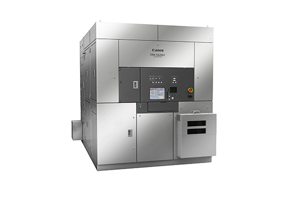
FPA-5520iV HR Option
As mobile devices become increasingly compact and energy-efficient, suppliers need to produce semiconductor chips that are thinner with a larger surface area. The market for semiconductor lithography equipment with greater FOWLP functionality continues to expand, reflecting increased demand for high-density redistribution layer wiring that requires high-resolution lithography.
While the FPA-5520iV achieves a resolution of 1.0 µm (micrometers3), the FPA-5520iV HR Option employs a new projection optical system that achieves a resolution of 0.8 µm, the finest resolution4 available in packaging-oriented lithography systems. This advancement allows finer circuit patterning to enable the further miniaturization of semiconductor chips while allowing increasing data bandwidth and processing speeds.
The FPA-5520iV HR Option maintains the same basic functionality, performance and productivity of the FPA-5520iV stepper (released in July 2016) for FOWLP processes while delivering a higher resolution of 0.8 µm. FPA-5520iV HR Option steppers provide improved productivity by offering such capabilities as handling extremely warped reconstituted wafers5, a problem encountered during mass production using FOWLP technology, as well as an improved rate of operation by automatic detection of alignment marks6 of chips that are known to be placed non-uniformly on reconstituted wafers.
By continuing to provide a wide variety of solutions and upgrade options for its semiconductor lithography equipment, Canon supports users' increasing productivity needs.
- 1A semiconductor lithography system that employs a 365 nm wavelength mercury lamp as the light source. 1 nm = one billionth of a meter
- 2Fan Out Wafer Level Package: A type of package technology that offers such merits as higher levels of integration, a greater number of external contacts and a smaller package footprint
- 3Micrometer (μm): 1μm = one millionth of a meter = one thousandth of a millimeter
- 4Among same-class i-line steppers. With flatness equal to Si wafer. As of December 10, 2018. Based on a Canon survey
- 5Wafers created by attaching and encasing in resin, multiple individual semiconductor chips that are produced during the front-end processes of semiconductor manufacturing.
- 6A system for performing alignment on a wafer surface, through observation and measurement of multiple alignment marks, vertical and horizontal positioning can be precisely determined.