News Release
Canon commences sales of the FPA-5520iV LF Option for back-end process semiconductor lithography systems that realizes a wide exposure field, supporting larger advanced packaging
TOKYO, February 2, 2021—Canon Inc. announced today the launch in Japan of the FPA-5520iV LF Option for back-end process semiconductor lithography systems, featuring an i-line stepper1 with a 1.5 µm (micrometer2) resolution and a wide exposure field of 52 mm x 68 mm for advanced packaging3.
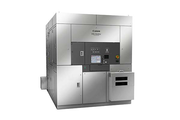
FPA-5520iV LF Option
In the field of semiconductor chip performance enhancement, alongside miniaturization of circuits in front-end process of semiconductor manufacturing, higher-density packaging in back-end processes is attracting greater attention. Advanced packaging that realizes high performance requires fine rewiring4, and in recent years, semiconductor lithography systems have been used for this purpose. Inheriting the same basic functionality of its predecessor model, the FPA-5520iV (released in July 2016), the new FPA-5520iV LF Option for advanced packaging achieves a wide exposure field of circuit patterns to meet a variety of advanced packaging needs including heterogeneous integration5.
Thanks to a new projection optical system, the Option realizes a single exposure with a large field of 52 mm × 68 mm—more than four times the standard exposure field (26 mm x 33mm) of front-end process lithography systems. This makes possible support for heterogeneous integration, in which multiple large semiconductor chips are bonded. In addition, with a high resolution of 1.5 µm, it is possible to expose fine rewiring patterns, thus supporting a variety of advanced packaging types. What's more, by introducing this high resolution option, rewiring patterns can be exposed with a high resolution of 1.0 µm.
The FPA-5520iV LF Option inherits the basic performance of the FPA-5520iV, which has received praise for its ability to handle warped reconstituted substrates6 an issue which can occur in packaging layers during the mass-production process, as well as high productivity to enhance availability by detecting alignment marks—even on the reconstituted substrates with large chip array variations.
- *1A semiconductor lithography system that utilizes a 365 nm wavelength mercury lamp as the light source. 1 nm (1 nanometer) = 1 billionth of a meter
- *21 µm (1 micrometer) = one millionth of a meter = one thousandth of a millimeter
- *3Protects delicate semiconductor chips from the external environment and allows them to be electrically connected to the outside at the implementation.
- *4Wiring for connecting between semiconductor chips or between semiconductor chips and bumps (protruding connecting electrodes).
- *5Packaging to combine different chips such as CPU and DRAM, or CPU and GPU. The chips can be placed close together and connected by a number of circuits to increase processing capability.
- *6Wafers created by attaching and encasing in resin multiple individual semiconductor chips that are produced during the front-end processes of semiconductor manufacturing.
The back-end process of semiconductor manufacturing
In the semiconductor chip manufacturing process, the semiconductor lithography system plays the role of "exposing" the circuit patterns. In the series of lithography processes, the process of forming a semiconductor chip on a silicon wafer is called the "front-end process." Meanwhile, the "back-end process" entails sealing a delicate semiconductor chip in a package, known as the "packaging process," to protect it from the external environment and to enable electrical connection with the external portion.
The Canon Lithography System website
The "Canon Lithography System Website" features easy-to-understand explanations, including illustrations and videos, of the technologies behind semiconductor lithography, as well as a dedicated page for kids.
URL: https://global.canon/en/product/indtech/semicon/50th/
Market trends in semiconductor lithography systems
The demand for various semiconductor devices is increasing due to the rapid progress of IoT in recent years, as well as an increase in remote work and online activities amid the ongoing COVID-19 crisis. Under such circumstances, high-density wiring of device packages has been proposed as an alternative to miniaturization in order to achieve high performance. It is predicted that the market for semiconductor lithography systems in the back-end process will continue to grow as the demand increases for advanced packaging that can support even higher-performance semiconductor devices. (Based on Canon research)