- Features
- Specifications
- Video
Basic Information
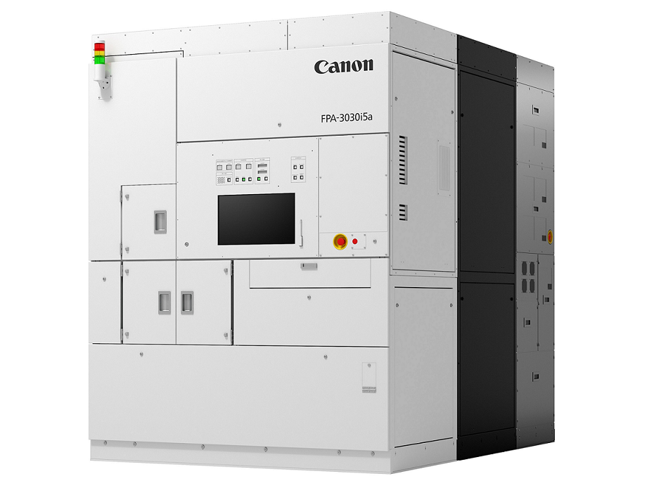
Model Name: FPA-3030i5a
Features
The FPA-3030i5a supports smaller substrates which are 200mm or less in diameter.
- *A wide range of wafer sizes from 50mm (2inch) to 200mm (8inch) are supported.
- *Approximately a 17% productivity improves compared to its predecessor model (FPA-3030i5+) under 8inch wafer condition.
- *The new chamber temperature control system helps to reduce power consumption by approximately 20% compared to its predecessor model (FPA-3030i5+).
- *Process robustness is enhanced by adopting an Off-Axis Alignment Scope that supports Dark-Field alignment measurement.
Supports a variety of different wafer sizes and materials
The FPA-3030i5a can be equipped with a handling system that enables the selection of wafer diameters from 50mm (2inch) to 200mm (8inch) to support a variety of different compound semiconductor wafer sizes and materials.
Adopts an alignment scope with enhanced robustness
The FPA-3030i5a employs an off-axis alignment scope that measures wafer alignment marks through an optical path that does not pass through the projection lens, which can use a wide range of alignment illumination wavelengths. And by enabling alignment measurement with Dark-Field can enhance process robustness.
TSA (Through Silicon Alignment) is also available as an option to support a variety of customer manufacturing processes.
Reduces Cost-of-Ownership through newly redesigned hardware and software
Productivity is improved by approximately 17% compared to its predecessor model (FPA-3030i5+) under 8inch wafer condition by adopting hardware such as a new alignment scope that shortens the measurement time of the alignment mark and a faster handling system, and by renewing the software.
And the power consumption is reduced by approximately 20% compared to its predecessor model (FPA-3030i5+) by adopting the new chamber temperature control system.
Specifications
| Resolution | ≦ 0.35 µm |
|---|---|
| Reduction Ratio | 1:5 |
| Field Size | 20mm x 20mm(5inch)/ 22mm x 22mm(6inch) |
| Exposure Wavelength | i-line 365 nm |
| Reticle Size | 5 inch / 6 inch (Selection) |
| Wafer Size | 50mm(2inch) / 75mm(3inch) / 100mm(4inch) / 150mm(6inch) / 200mm(8inch) (Selection) |
| Overlay Accuracy | ≦ 40 nm |
| Main Body Dimensions | (W) 1,900× (D) 2,600× (H) 2,450mm (Included exhaust duct: 2650mm) |
| Major Options | Wafer Handling Kit for Special Substrates PC Remote Console GEM-compliant online software Pellicle Particle Checker Through Silicon Alignment |
Video
*In order to view videos, it is necessary to consent to the use of cookies by our website. If the videos are not displayed, please click the "Cookie Settings" and accept cookies.