- Features
- Specifications
Basic Information
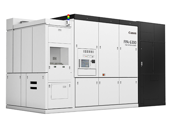
Model Name: FPA-6300ESW
Features
FPA-6300ESW scanners are equipped with a Wide-Field Lens
By changing the projection lens magnification (4:1 → 3.125:1), FPA-6300ESW scanners realize a wider exposure field with the reticle size remaining at 6 inches.
The FPA-6300ESW is the only KrF scanner in the world that can expose a full size CMOS image sensor without *stitching because 33 mm x 42.2 mm can be exposed in one shot.
- * Stitching exposure: A method of increasing exposure field size by connecting two or more adjacent exposure regions. The positional accuracy and alignment of the adjacent exposure regions directly affects the yield.
FPA-6300ESW scanners are derived from the proven FPA-6300ES6a Platform
FPA-6300ESW scanners adopt technology developed to support Front-End-Of-the-line (FEOL) semiconductor manufacturing processes and are able to provide the similar utilization and reliability as FPA-6300ES6a scanners.
FPA-6300ESW scanners also feature an extendable platform allowing field upgrades for improving productivity and overlay accuracy.
Specifications
| Resolution | ≦ 130 nm |
|---|---|
| NA (Numerical Aperture) | 0.45~0.70 (Variable) |
| Reduction Ratio | 1:3.125 |
| Field Size | 33 mm x 42.2 mm |
| Exposure Wavelength | KrF 248 nm |
| Reticle Size | 6 inch |
| Wafer Size | 300 mm (12 inch) |
| Overlay Accuracy | ≦9nm |
| Main Body Dimensions | (W) 2,300 x (D) 5,155 x (H) 2,900 mm |
| Major Options | AFIS Illumination System SMIF OHT Kit PC Remote Console GEM-compliant online software Pellicle Particle Checker |