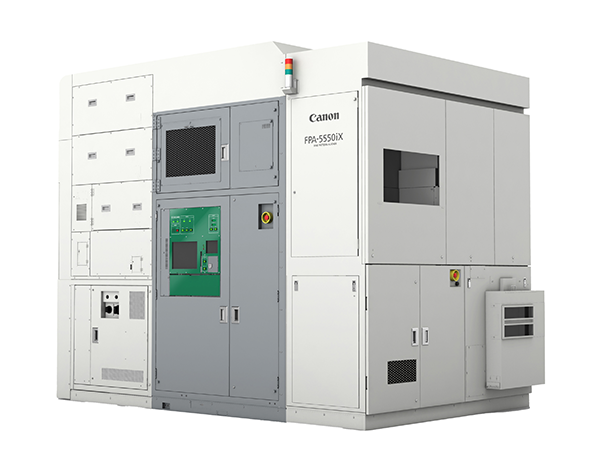
FPA-5550iX
Wide-Field / High Resolution i-line Stepper
- Features
- Specifications
Basic Information
Model Name: FPA-5550iX
Features
The FPA -5550 iX utilizes the same projection lens used by its predecessor model, the FPA -5510 iX (released in September 2015) which enables a high resolution of 0.5μm. Thanks to a wide exposure field of 50 x 50 mm, the system can perform high-resolution single exposure for full-frame CMOS sensors, next-generation displays for XR devices and more. What’s more, manufacturing processes have been refined to ensure high-quality, stable production of projection lenses, many of which are used in the system, to meet the strong demand expected for semiconductor lithography systems.
In addition, a new alignment scope that can read wider variety of alignment marks* has expanded the range of processes in which FPA -5550 iX can be used. In addition to the "bright-field detection" function for measuring direct light, a new "dark-field detection" function has been added to the alignment scope, enabling the measuring of scattered and diffracted light, thus allowing users to select a wide range of measurement methods. Low-noise measurement has been made possible by expanding the range of usable wavelengths while also employing an area sensor for multi-pixel measurement. Thanks to these advancements, the system can detect and measure low-contrast alignment marks. What’s more, the system can optionally select an infrared wavelength that can pass through silicon, enabling users to measure the alignment on the back of the wafer, which is a requirement for the manufacture of back-illuminated sensors. The flexibility of alignment mark measurement thus allows the system to be utilized in a variety of processes.
- * Marks placed on silicon wafers to secure accurate circuit pattern overlay
When combined with Canon’s Lithography Plus solution platform (released in September 2022), the FPA -5550 iX, provides operators with the ability to monitor the condition of the lithography system, as well as perform analyses, helping them maintain appropriate quality control and higher utilization rates.
Specifications
| Resolution | ≦ 500 nm |
|---|---|
| NA (Numerical Aperture) | 0.37~0.28 (Variable) |
| Reduction Ratio | 1:2 |
| Field Size | 50 mm x 50 mm (Φ70.7 mm inside) |
| Exposure Wavelength | i-line 365 nm |
| Reticle Size | 6 inch |
| Wafer Size | 300 mm (12 inch) |
| Overlay Accuracy | ≦ 50 nm |
| Main Body Dimensions | (W) 2,300 x (D) 3,660 x (H) 3,000 mm |
| Major Options | Chemical Filter Resist Outgas Exhaust Unit PC Remote Console GEM-compliant online software Pellicle Particle Checker Enhanced AGA (EAGA, shot-by-shot overlay) Through-Silicon Alignment Scope (TSA-Scope) |