






News Release
November 10, 2026
Canon Inc.
Canon launches FPA-6400ES6a KrF semiconductor lithography system with high throughput and industry-leading overlay accuracy
TOKYO, November 10, 2026—Canon Inc. today announced that it will launch the FPA-6400ES6a, a new KrF1 scanner for semiconductor manufacturing applications including memory and logic devices, in early December 2026.
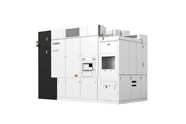
Demand for advanced semiconductors is growing amid the expanding use of generative AI, increasing the need for greater productivity in semiconductor manufacturing. At the same time, the shift toward more highly integrated devices is leading to a greater number of exposure processes and the use of multilayer structures, making wafer warpage and distortion more pronounced. Semiconductor lithography systems must therefore not only process more wafers, but also maintain precise pattern overlay under increasingly demanding manufacturing conditions. The FPA-6400ES6a addresses these requirements with a throughput of 400 wafers per hour,2 industry-leading overlay accuracy of 4.0 nm,3 and greater flexibility to accommodate diverse semiconductor manufacturing processes. A newly developed ultra-high-acceleration stage reduces stage travel time, enabling a significant improvement in productivity over the previous model,4 while newly developed vibration-suppression technology helps achieve the system's industry-leading overlay performance. Combined, these advances help boost productivity and improve yield in advanced semiconductor manufacturing.
Canon has also added a new light source, the High Alignment Light Source (Hi-ALS), as an option for its proprietary image alignment system. Users can select the alignment measurement wavelength to suit different semiconductor manufacturing processes, enabling highly precise alignment. The system provides enhanced wafer holding capability and accommodates wafer warpage of up to 700 μm, thereby improving its ability to handle warpage arising from the multilayer structures of three-dimensional devices and wafer bonding processes.4
The FPA-6400ES6a also incorporates newly developed technology that stores regenerative power generated when the wafer stage decelerates and reuses it as needed, as well as a high-efficiency power supply developed to support the ultra-high-acceleration stage.
- 1.
Krypton fluoride. The exposure wavelength is 248 nm.
- 2.
The number of 300 mm wafers exposed per hour under conditions of 96 shots per wafer
- 3.
Among KrF scanners for 300 mm wafers, as of November 9, 2026. Based on Canon research
- 4.
Compared with the previous FPA-6300ES6a model, launched in April 2012, when equipped with optional features