






Nanoimprint Lithography
Optimizing Mass Production Lines
in Semiconductor Manufacturing
Semiconductor manufacturing relies on exposure, a process that transfers circuit patterns onto silicon wafers. As circuit miniaturization advances in response to demand for increased data-processing capacity, challenges associated with traditional optical lithography, such as high power consumption, are becoming increasingly pronounced. To address these issues, Canon developed Nanoimprint Lithography (NIL) as a next-generation technology. Following the launch of NIL-equipped systems in 2023, customers who have adopted this equipment have been making final adjustments in order to optimize mass production lines for semiconductor manufacturing. We spoke with two engineers at the forefront of this effort about their journey so far and their future outlook.
- (This article is based on information available at the time of writing.)
Table of Contents

Optical Products Operations
Takahiro Sato
Takahiro Sato joined Canon in 2010. After gaining five years of experience in semiconductor device development, he was transferred to the semiconductor equipment development division to research how device characteristics affect manufacturing equipment. He is currently focused on equipment evaluation and process development in an aim to improve overlay accuracy in the lithography process.

Optical Products Operations
Masato Shichijo
Masato Shichijo joined Canon in 2020 and was immediately assigned to work on NIL. Leveraging his academic background in electrical and electronic engineering, Shichijo currently oversees control design from both electrical engineering and software development perspectives. He uses his unique role in bridging hardware and software end-to-end to fully concentrate on system-wide optimization.
Expectations and Challenges for NIL
What is the crucial difference between conventional optical lithography and NIL?
If we think of optical lithography as "projecting shadows with light," NIL is almost like "stamping." The most distinctive feature of NIL is a template, called a “mask,” engraved with circuit patterns and pressed directly onto the resin applied to the wafer. This allows complex structures to be formed all at once in a single step, eliminating the need for repetitive exposures which are required in conventional optical lithography. Also, because NIL doesn’t use a light source to form circuit patterns, it offers the significant advantage of reducing power consumption to approximately one-tenth that of conventional methods.
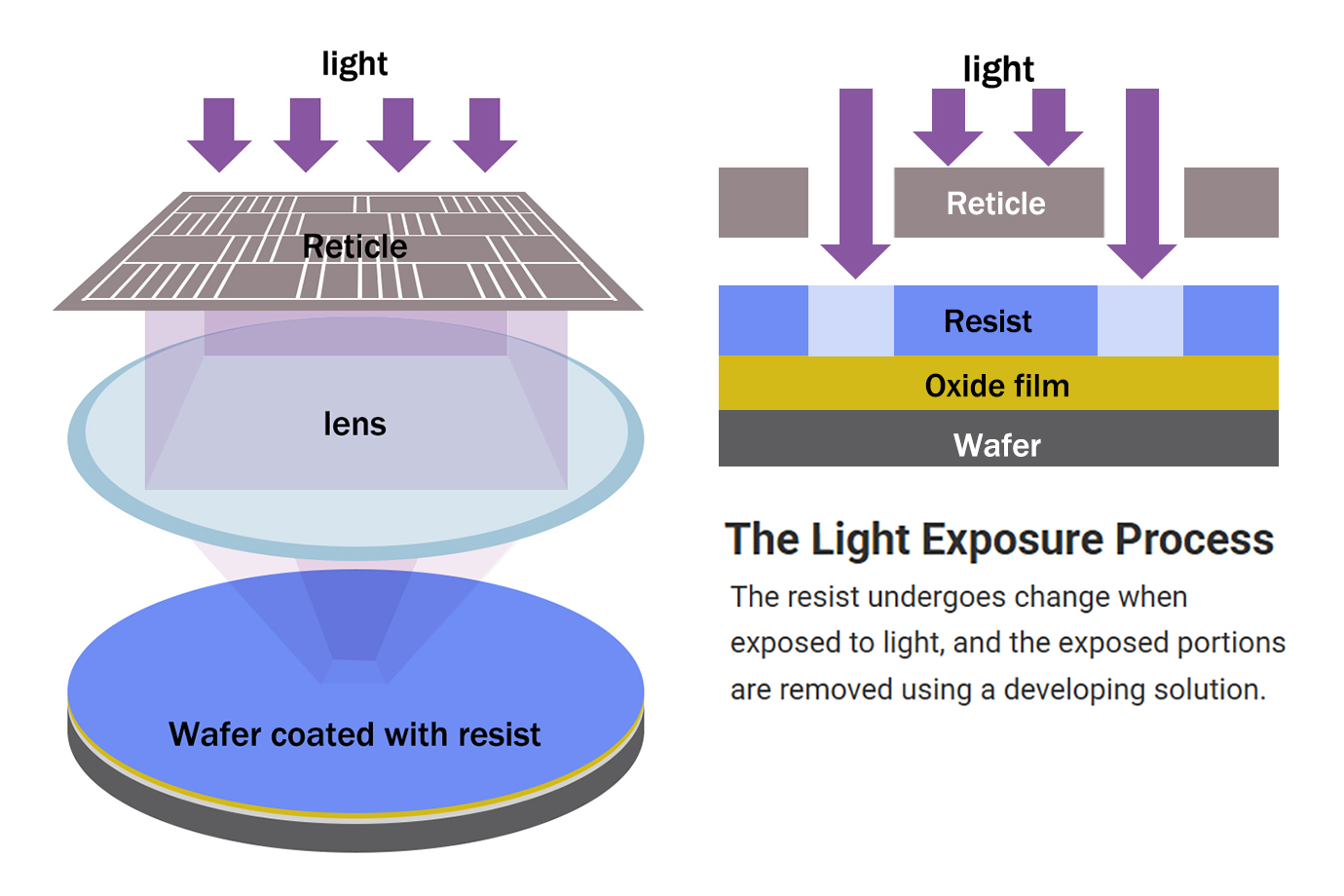
For details, please visit Canon's technology page on "Nanoimprint Lithography."
On the other hand, direct contact between the mask and the wafer poses challenges that are unique to NIL. Since semiconductor chips are manufactured by stacking multiple layers, ultra-high overlay precision at the nanometer level is absolutely necessary. In addition, if particles—meaning foreign contaminants—get trapped during contact, they can cause defects or damage the mask. We tackled these issues one by one through continuous trial and error.
Tackling Engineering Challenges
Could you share a particularly difficult episode from your trial-and-error process?
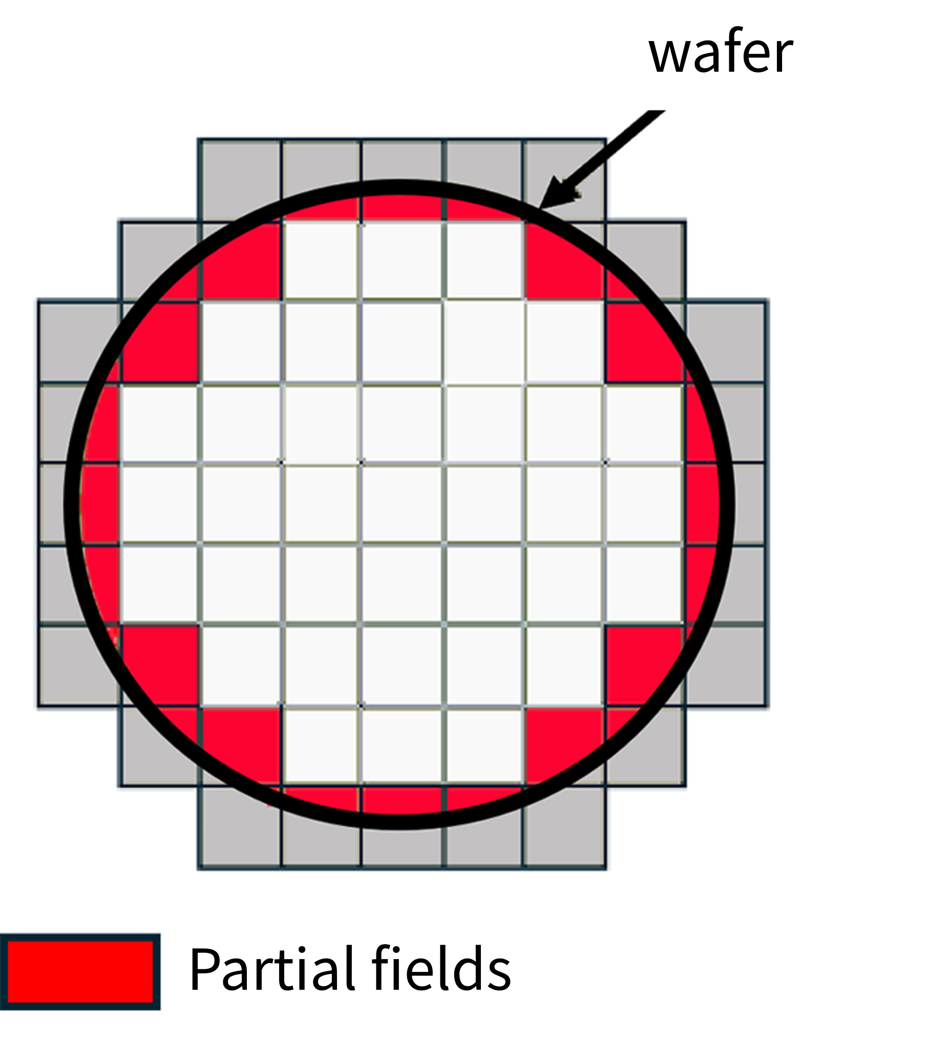
Processing the wafer edge, known as the "partial field," was a critical issue for development. Due to the structural issues that arise from using square masks on circular wafers, contact tends to become unstable around the perimeter. One of the biggest challenges was designing the process to ensure that the pattern transfer could be performed just as accurately as with conventional technologies, while taking into account not only boundary condition settings but also the effects of post-processing steps—such as etching to remove excess patterns and processes that impart electrical characteristics.
Personally, I faced a major hurdle in achieving the target transfer accuracy specified in the design during high-volume manufacturing. After analyzing vast amounts of data for over a month, I identified the root cause of subtle errors and resolved the issue through hardware refinements.
We also struggled greatly during discussions with our U.S. affiliate, our partner in NIL R&D. Discussions were conducted entirely in English, so I was initially intimidated by technical conversations full of specialized jargon. However, I came to realize that I was the person most familiar with customers' on-site needs. With that perspective, I began proactively making proposals and contributing to discussions with greater confidence. This helped me gain the support and understanding of those involved and dramatically sped up the development process.

Future Outlook
What is needed to optimize mass production lines in semiconductor manufacturing using NIL?
Our customers cannot operate NIL fully as a standalone system. While working closely together with group companies to enhance precision for use in semiconductor manufacturing equipment, we must optimize the entire manufacturing process, including peripheral equipment such as mask cleaning systems.
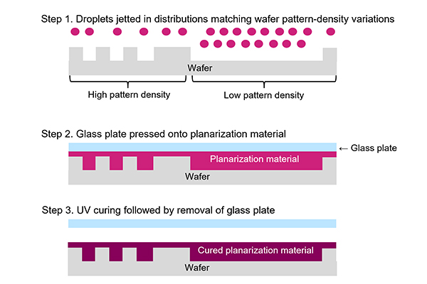
At the same time, we must identify issues directly at customer sites. When it comes to semiconductor manufacturing, subtle surface topographies on the wafer—arising during repeated deposition and wiring steps—can lead to alignment errors and impact productivity. Therefore, we applied NIL as a planarization technology called Inkjet-based Adaptive Planarization (IAP) to flatten wafer surface topographies uniformly. Going forward, the key to bringing NIL into practical use will be expanding its range of applications while tackling the challenges faced at manufacturing sites.

What are your future goals?
NIL is finally entering the final stage: full-scale adoption for mass production at customer sites. Completing this mission is our responsibility, and I am convinced that its success will directly lead to energy savings throughout society and accelerate further technological evolution.

Our next milestone is bolstering overall capability required for mass production processes. By thoroughly extending mask life and reducing costs, we aim to refine the technology to a level where customers can operate it just as easily as conventional equipment. While our technical capability in NIL is currently one step ahead of competitors, enhancing our performance in mass production processes remains an ongoing challenge. Because there is no precedent, we have the opportunity to change the world with our own hands. I want to explore uncharted territory alongside colleagues who share that same passion.
Behind the Scenes of Development:A workplace where taking on challenges becomes your role
At Canon, we have an open environment where employees can actively submit patent applications regardless of tenure or age. If a proposal is recognized—demonstrating how solving a specific issue brings clear benefits to the customer—you may even be appointed as a project leader. The ability to take initiative in an encouraging culture, help shape the workplace atmosphere, and experience personal growth day by day is one of the best aspects of my job.
On the front lines of engineering, there are often "gray areas" where ownership is not clearly defined. In those moments, we bring the relevant teams together, identify the issues at hand through facilitation, and map out a path to a solution. For those who find joy not just in completing assigned tasks, but in conducting independent research, there is no place more rewarding to work than Canon.
