





Technologies that support products
Device Platform
- A technology platform that organizes technologies built through the development and manufacturing of key devices
- Contributes to the development of high-value-added products by continually advancing core technologies, such as photoelectric conversion
- Further shortens new-product development lead times through company-wide deployment across a wide range of product categories
Table of Contents
What is the Device Platform?
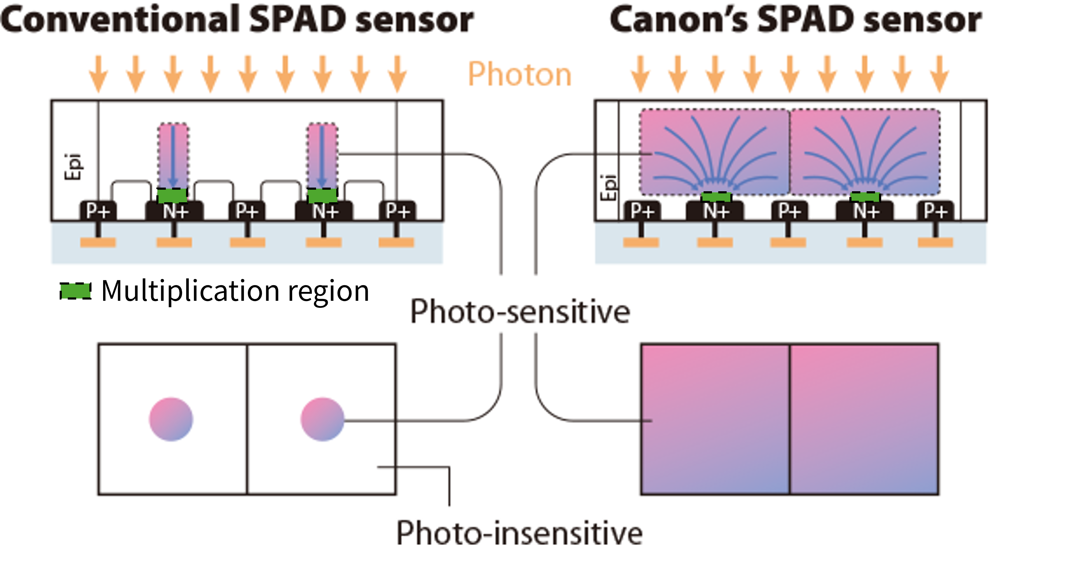
Canon's Device Platform organizes the technologies Canon has accumulated through the development and manufacturing of key devices so that they can be utilized throughout the entire company. Semiconductor devices serve as the critical control, processing, and conversion hubs of our products, actively giving shape to product functions and performance. Consequently, the capabilities and quality of these semiconductor devices significantly impact the overall value of the end products.
For many years, Canon has refined its technical foundation which is essential for semiconductor device development and production. In particular, by continuing to evolve technologies such as photoelectric conversion, MEMS, and light-emitting material deposition, we have consistently generated high-value-added products.
We have arranged these technologies and know-how into a company-wide device platform. By directly connecting the key devices at the core of our products to in-house mass production, we continue to enhance the competitive edge of our products. For example, Canon applies technologies cultivated through the development of camera sensors to develop and reliably supply image sensors capable of capturing subjects in environments with significantly different levels of brightness, such as dark roads at night and tunnel exits. Canon also rapidly deploys advanced technologies developed for electronic viewfinders in cameras across a wide range of products, including commercial digital presses and multifunction devices, thereby enhancing the performance of new products and shortening development lead times.
Case study:High-sensitivity SPAD sensor leveraging technologies cultivated through CMOS sensors
Photoelectric conversion technology is, quite literally, the technology that converts light into electrical signals, which Canon has cultivated through the development of products like CMOS sensors. Applying this photoelectric conversion technology, Canon has developed a SPAD sensor based on operating principles different from those of conventional CMOS sensors.
- *For details, please visit our technology page on SPAD sensors.
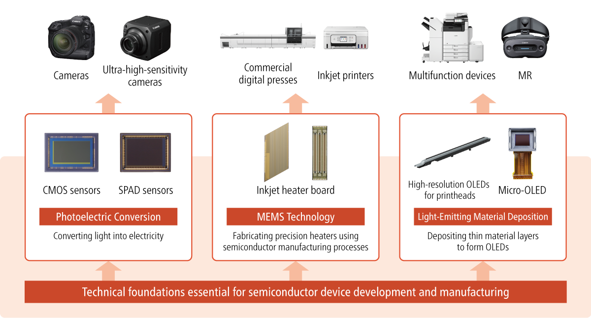
In SPAD sensors, the design of the light-receiving region and the multiplication region significantly impacts overall performance. In conventional SPAD sensors, these regions were integrated into a single structure. As a result, expanding the light-receiving area also enlarged the multiplication region, which introduced noise into the signal.
Applying the pixel design technologies accumulated through CMOS sensor development, Canon created a proprietary pixel architecture that optimizes both the light-receiving and multiplication regions. Consequently, this design achieves both high sensitivity and low noise, maintaining a large light-receiving area while keeping the multiplication region small.
As a result of this proprietary pixel architecture, Canon’s SPAD sensor achieves both high sensitivity and high pixel density—enabling it to detect a pedestrian 120 meters away, even in low-light environments of 0.1 lux.*
Thanks to these unique characteristics, the sensor is expected to be utilized across a wide variety of fields, including surveillance, automotive, industrial, and medical equipment.
- *For reference, the brightness of a moonlit night is approximately 0.2 lux.
Case study:Exposure system for multifunction devices applying OLED technology developed for electronic viewfinders
Canon independently developed OLEDs for the electronic viewfinders of interchangeable-lens cameras, achieving high brightness, high pixel density, and high luminous efficiency. By organizing this technology as a device platform, Canon is able to expand its application to products beyond cameras. One example is its deployment in the exposure system of office multifunction printers.
Conventional office multifunction printers reproduced text and images using a process where laser light altered charge states based on print data—creating invisible electrical patterns on which toner was deposited. The dominant conventional exposure method used mirrors to scan a laser beam at high speeds, exposing the drum line by line to draw images. While this approach enabled high-precision image formation, its reliance on mechanical components, such as rotating mechanisms, imposed constraints on miniaturization and further resolution enhancement.
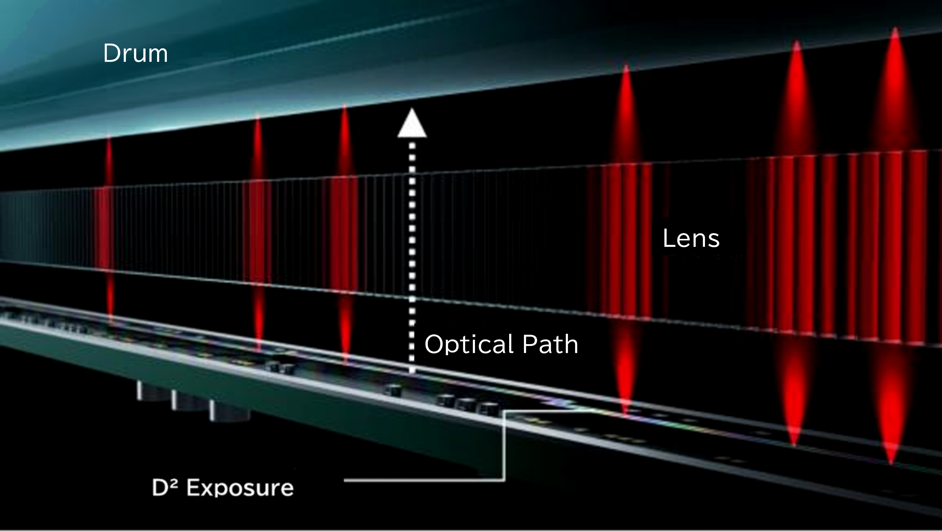
To address these challenges, Canon developed "D2 Exposure," a novel exposure method that utilizes OLED technology. OLEDs emit light when an electric current is applied, allowing precise light control at the individual micro-pixel level. Leveraging this characteristic, Canon moved away from the conventional approach of drawing images with moving light, enabling one-shot exposure via light-emitting elements arrayed in a line.
This construction resulted in a more compact design while simultaneously delivering both high resolution and high speed. Furthermore, by precisely controlling these densely arrayed light-emitting elements, Canon also attained exceptional rendering quality.