







Producing semiconductors indispensable for our daily lives
Semiconductor Lithography Equipment
Automobiles, smartphones, home appliances, and other devices that are indispensable for our daily lives contain many semiconductors.Demand for semiconductors, particularly those used for generative AI and automated driving, is rapidly increasing. Semiconductor lithography equipment, which is essential for semiconductor production, requires the world's most advanced optical and control technologies.
Table of Contents
Overview of Semiconductor Lithography Equipment
What is a semiconductor?
Semiconductors are substances such as silicon that have properties intermediate between conductors, such as metals, which conduct electricity well, and insulators, such as rubber and plastic, which conduct little electricity.
"Semiconductors" collectively refer to transistors1 and integrated circuits2 that use semiconductors as materials.
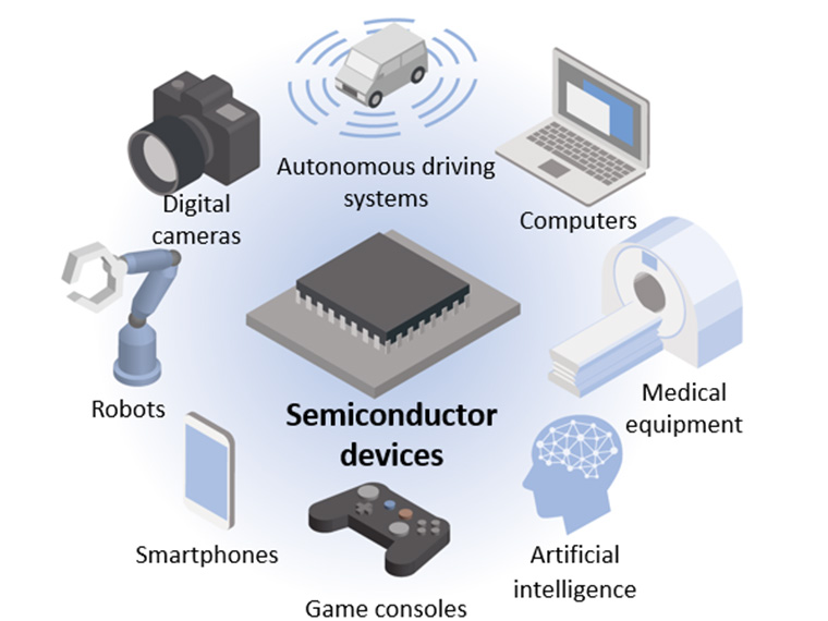
- 1. Electronic elements that amplify or switch electrical signals
- 2. A circuit in which many transistors are integrated and wired together
The Semiconductor Chip Manufacturing Process
The semiconductor chip manufacturing process can be broadly divided into three processes.
- The design process, in which the wiring circuits are designed
- The front-end process, in which electronic circuit patterns such as transistors and wiring are transferred to a semiconductor wafer through exposure
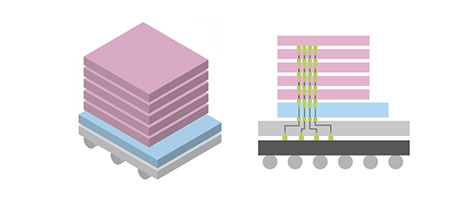
- The back-end process, in which wafers with electronic circuits formed on them are divided into individual chips and assembled
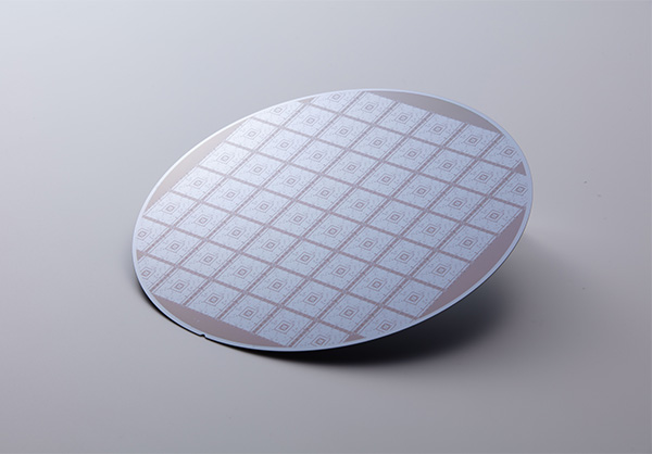
[Front-end processing]

[Back-end processing]

Semiconductor lithography equipment has mainly been used in front-end processes.
However, the performance improvement of semiconductors through the miniaturization of circuit patterns in the front-end process is approaching its limit. Instead, using semiconductor lithography equipment in the back-end process as well, efforts are being made to connect multiple semiconductor chips with high-density wiring into a single large-scale semiconductor using what is called 3D integration technology.
Overview of Semiconductor Lithography Equipment
Semiconductor lithography equipment projects fine circuit patterns onto wafers.
The equipment consists of an illuminator that produces bright and uniform light suitable for exposure, a reticle stage on which a reticle is placed, a projection optical system consisting of many lenses, a wafer stage on which a wafer is placed for exposure, and an alignment scope that measures the wafer mounting position.
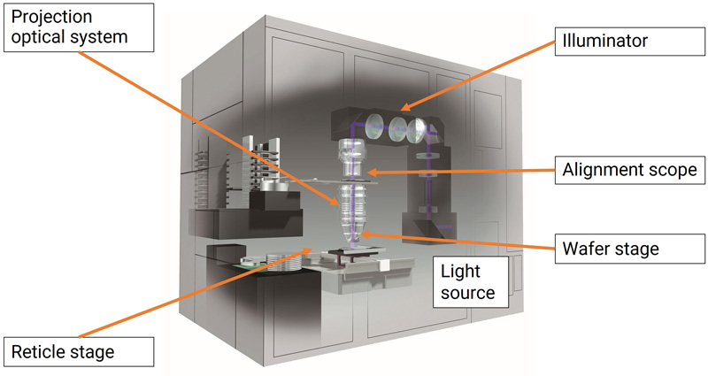
Semiconductor lithography equipment transfers circuit patterns to wafers through the following process.
- First, the wafer is placed on the wafer stage. The alignment scope is used to correctly position the wafer.
- A reticle with a circuit pattern is placed on the reticle stage.
- Ultraviolet (UV) light is illuminated from above.
- The UV light passing through the reticle passes through the projection optical system to project the circuit pattern of the reticle onto the wafer placed on the wafer stage.
A resin, called the "photoresist," has been applied to the surface of the wafer in advance. This photoresist changes when it is exposed to UV light, so the electronic circuit pattern on the reticle is transferred.
Types of semiconductor lithography equipment
In general, the types of semiconductor lithography equipment are categorized by the light source: i-line, KrF, ArF, and EUV.
In addition to ArF, the ArF immersion method, which can form a finer circuit pattern by filling the space between the lens and wafer with pure water, which has a higher refractive index than air, is categorized separately.
Canon's nanoimprint semiconductor lithography equipment*1, on the other hand, cannot be classified by light source, as it uses a completely different mechanism than conventional lithography equipment. The line width of the circuit that can be formed is very narrow, so it can also be adapted to state-of-the-art semiconductor manufacturing.
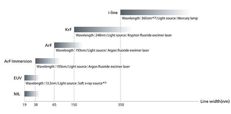
-
*1 Circuits are formed using a simple principle that involves transferring a circuit pattern mask (mold) onto the coated photoresist on the surface of the wafer.
See "Nanoimprint Lithography" for details. - *2 nm = nanometer, or 1/1,000,000,000 of a meter
- *3 X-rays of longer wavelength
The Three Main Performance Characteristics of Semiconductor Lithography Equipment
The following three performance characteristics have the greatest impact on the performance of semiconductor lithography equipment.
1.Resolution
Resolution is a measure of how fine the circuit patterns that are transferred (via exposure) to the wafer can be. Generally speaking, the finer the circuit pattern, the more compact the resulting semiconductor chip and the greater its performance. This in turn improves the performance of the products containing the semiconductor chips.
2.Overlay accuracy
Each wafer is exposed multiple times to create numerous circuit patterns. Overlay accuracy indicates how precisely wafers and reticle circuit patterns can be overlaid. This characteristic is directly linked to semiconductor chip yield rates.
3.Throughput
This refers to the speed with which wafers can be processed, and is an indicator of production efficiency. It is an important indicator for mass production intended to manufacture as many semiconductor chips as possible within a given amount of time.
Canon’s semiconductor lithography equipment
Design, Manufacture, and Control Technologies Used in Projection Lenses with Higher Resolutions
Extraordinary Aberration Control for Achieving Theoretical Resolution Limits
The circuit pattern drawn on the reticle is reduced by a projection lens and exposed onto the wafer.
The greater the resolution of the projection lens, the more delicate the patterns can be, increasing the circuit density.
Projection lens are manufactured using Canon's advanced optical design, assembly, and adjustment technologies, as well as lens polishing technology with a precision of several nanometers, both developed through the manufacture of cameras.
In addition, the resolution is enhanced by a mechanism in which the lens driver compensates for aberrations caused by slight environmental changes such as atmospheric pressure and temperature.
Semiconductor lithography equipment continues to operate 24 hours a day, 365 days a year. Over time, the circuit pattern passing through the lens becomes blurred or distorted due to heat during exposure and aging.
Canon developed projection lens that reduces distortion in projected circuit patterns by reviewing lens materials. The equipment can transfer accurate circuit patterns down to nanometers and can produce high-quality semiconductor chips.
Using Big Data Analysis Technology to Support Stable Operation
A support system to keep the equipment running is essential.
The semiconductor lithography equipment business is not completed when products are delivered to customers' factories.
It is important to have the customer-supporting technology to constantly maximize the performance of the equipment while it operates 24 hours a day, 365 days a year in the factory, to ensure customers' high productivity and exposure accuracy.
To this end, Canon developed a platform system that leverages its know-how in supporting equipment operation and the vast amount of data on semiconductor manufacturing processes, including the exposure process.
It supports stable operation of the equipment by automatically detecting abnormalities and restoring them by making full use of analysis technology for the enormous data accumulated.