Vacuum thin-film deposition equipment essential for semiconductor manufacturing
Sputtering Equipment
With the rapid advancement of generative AI, demand for semiconductor devices—especially those used in data centers—is increasing. Sputtering equipment supports semiconductor manufacturing by enabling high-quality, high-precision film deposition using advanced vacuum technologies.
Table of Contents
How sputtering equipment works
What is sputtering equipment?
Sputtering equipment is used to form thin films on a wafer to create circuits for semiconductor devices. It is typically used in the production of Semiconductor devices, which are seeing growing demand in fields such as generative AI and the automotive industry.
The manufacturing process of semiconductor chips is divided into two stages: the front-end process, where electronic circuit patterns are formed on a wafer, and the back-end process, where the patterned wafer is cut into individual chips and assembled to function properly within electronic devices.
Among the various semiconductor manufacturing systems, sputtering equipment is primarily used in the front-end process to deposit thin films onto the wafer. A single semiconductor chip may contain over thirty layers of film, with each layer requiring highly precise deposition technology—some as thin as 1 nanometer (nm), which is one-billionth of a meter.
Front-end processing

Back-end processing

What is the sputtering phenomenon?
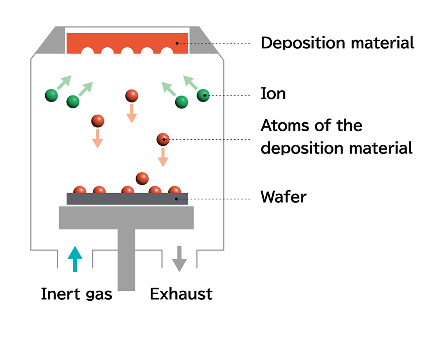
Sputtering is a phenomenon in which electrically charged atoms (ions) collide at high speed with the surface of a material, causing atoms or molecules to be ejected. Inside the sputtering equipment, the target material (film deposition material) and the wafer on which the thin film is to be formed are placed in a vacuum chamber. When an inert gas is introduced into the chamber and a voltage is applied to the target, the atoms ejected from the target material adhere to the wafer, forming a thin film that constitutes the circuit.
Thin films exhibit various electrical properties depending on the materials used, their shape, and thickness. These properties are utilized in semiconductor devices such as memory for data storage, logic circuits—the brain of computers—LEDs for lighting, and various sensors.
- * Inert gases are chemically stable and do not easily react with other substances. Argon (symbol: Ar) is commonly used in semiconductor manufacturing due to its low reactivity.
- * In order to view videos, it is necessary to consent to the use of cookies by our website. If the videos are not displayed, please click the "Cookie Settings" and accept cookies.
What is an ultra-high vacuum?
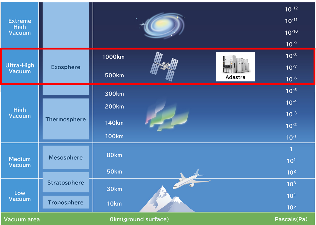
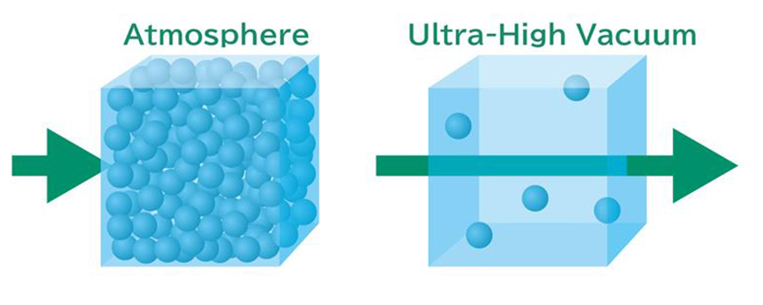
Sputtering is performed in an ultra-high vacuum environment. “Ultra-high vacuum” refers to a state of pressure that is less than one-ten billionth of that on the Earth's surface, comparable to the pressure at the altitude of 400 km where satellites such as the International Space Station orbit. During film formation, countless gas molecules in the atmosphere can act as obstacles or impurities. By creating an ultra-high vacuum—a rarefied environment with very few gas molecules—it becomes possible to release atoms and molecules into space exactly as intended, thereby enabling the formation of thin films with minimal impurities required for semiconductor applications.
Canon's Sputtering Technology
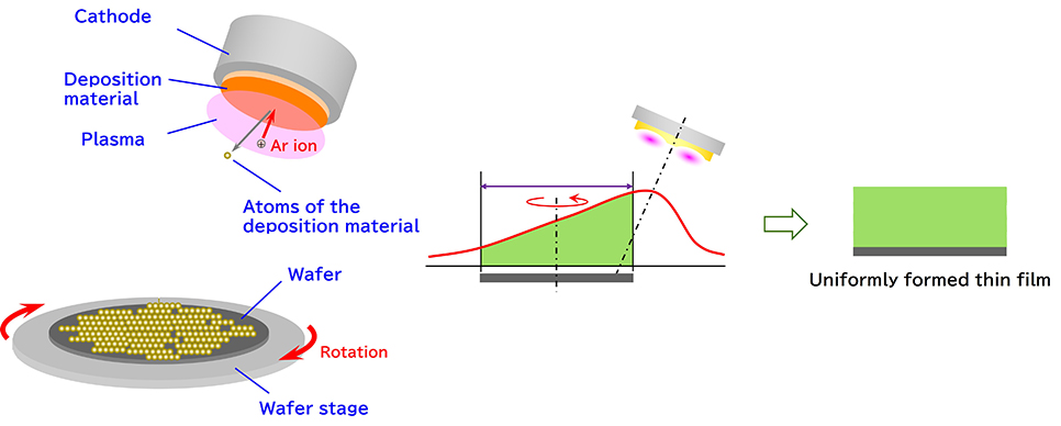
Oblique sputtering with rotating substrate: A technology for uniformly forming ultra-thin films of less than 1nm
Oblique sputtering with rotating substrate is a technique in which the cathode electrode that generates plasma is positioned at an angle to the wafer surface, and the substrate stage rotates during film deposition. This allows for uniform film formation and precise control of film thickness, enabling the creation of extremely thin films. Multiple pieces of target material can also be arranged, making it possible to build films with over thirty layers using different materials.
This technology contributes to the production of various semiconductor devices, including non-volatile memory* that supports energy-efficient operation.
- * Memory that retains data even when the power is turned off, such as USB flash drives, SSDs, and contactless IC cards
Application to atomic diffusion bonding technology
In semiconductor device manufacturing, technologies that enhance performance by bonding wafer together are advancing. Canon's atomic diffusion bonding system enables this by utilizing sputtering technology to form a thin bonding layer on the surfaces of the wafer.
During bonding, atoms at the interface rearrange themselves according to the atomic structure of the opposing surface—a phenomenon known as atomic diffusion. This results in a bond so strong that the boundary between the materials becomes nearly indistinguishable.
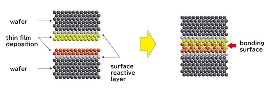
Right: Robust bonding achieved through atomic diffusion
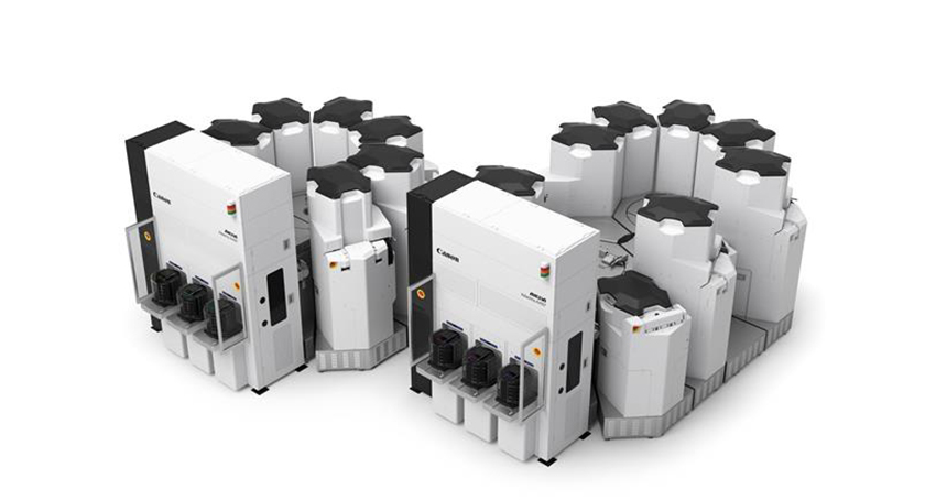
Adastra is a sputtering system that offers flexible configuration options tailored to the semiconductor devices being produced, allowing it to meet a wide range of needs. In the semiconductor industry, where both productivity and environmental considerations are essential, Adastra enables nano-level thin film deposition while minimizing space and energy consumption.
Its design and usability have been highly praised, earning it the Gold Award in Japan's 2024 Good Design Awards and the top prize (Minister of Economy, Trade and Industry Award) at the 55th IDEA Machine Industry Design Awards. Internationally, it also received the Gold Award at Germany's 2025 iF Design Awards in recognition of both its technological excellence and design quality.