
The World's First Million-Pixel SPAD Sensor*: The Product of an Engineer's Relentless Inquisitiveness
A SPAD sensor is a unique type of imaging sensor that can capture extremely fast-moving objects, including even light particles. Canon engineer Kazuhiro Morimoto realized its benefits very early on, and went on to develop the world's first one-million-pixel SPAD sensor after studying abroad in Switzerland. In doing so, he opened up new possibilities in imaging. Here he tells us his story.
- *Out of SPAD sensors. As of June 23, 2020. Based on Canon research
Canon develops world's first 1-megapixel SPAD image sensor
Table of Contents

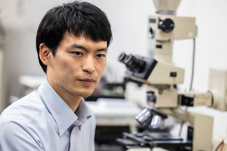
Kazuhiro Morimoto
Senior Engineer, Device Technology Development Headquarters
Morimoto became interested in Canon because he loved the Canon cameras that he used for his stargazing hobby. He joined Canon in 2013, and since then has been involved in the development of image sensors. UK-based scientific journal Nature named him one of the four “rising stars who are reshaping nanoscience” following his groundbreaking achievements in SPAD sensor development.
An encounter with the unknown The sensor that almost no one had ever heard about
I found out about SPAD (Single Photon Avalanche Diode) sensors soon after I joined Canon in 2013. I was part of a team developing CMOS image sensors, which are widely used in cameras, and a mention of SPAD sensors in a paper I was reading for research caught my attention. I was fascinated by this sensor that was said to “capture images using principles completely different from that of a CMOS sensor” and became more enthralled as I read more research papers about it.
What was it about SPAD sensors that drew you to them?
SPAD sensors are fascinating because their mechanism can count individual photons (light particles), which are the smallest unit of light. As they can also amplify a photon by as much as 1 million times in an instant, with very little noise introduced during amplification, I had the feeling that they held tremendous potential for image capture in dark environments, such as at night.
I love physics. I have been interested in Albert Einstein's theory on the dual nature of light (wave-particle duality) since high school, and believed that researching SPAD sensors would allow me to gain a deeper understanding of this subject.
Canon had already accumulated a vast amount of technology related to CMOS sensors, which I had been working on since I joined the company, through many years of research by many engineers. Therefore, I thought it would be difficult for me to make substantial further contributions, even if I were to catch up to the established technology. I kept thinking about how I could contribute to the company, and eventually hit on the idea of creating my own new SPAD sensor technology.
Back then, hardly anyone in the company had heard of the term “SPAD.” I proposed the idea of launching research and development of SPAD sensors to my superiors and began surveying technologies. I was alone at first, but I convinced the people around me of its potential and the necessity of research. Gradually, more people became involved, and our research began to pick up speed.
Training at one of the most advanced institutions Going for further studies in Switzerland, home of the world's most advanced SPAD research
I had wanted to work overseas since I joined the company. After encountering SPAD sensors, I began to believe that SPAD research should be conducted in cutting-edge academic institutions. That is why I chose to enter a university abroad.
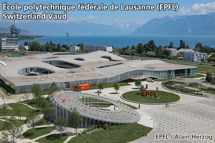
I went to the École Polytechnique Fédérale de Lausanne (EPFL), which has been known to conduct some of the most cutting-edge research on SPAD sensors. In 2003, the researchers there developed a SPAD sensor for the first time in the world using the same mass-production type semiconductor manufacturing process that is used to produce CMOS sensors.
How did you conduct research at EPFL?
The research topic that I was given when I enrolled was to “develop a 1-megapixel SPAD sensor,” something that no one in the world had accomplished at that time. My research supervisor, Professor Charbon, gave me a general vision, but how I conducted my research was basically all up to me.
At Canon, consultations with our superiors are part of the everyday work culture. However, at EPFL, even if we did discuss the project with our professors and get ideas from them, the general style was “figure it out yourself.” I was a little lost at first, but throughout the entire trial-and-error process, I gradually learned to enjoy identifying problems and finding solutions to them on my own.
Realizing my mentor's dream Successfully developing the world's first million-pixel SPAD sensor
When I first started at EPFL, one of the fundamental challenges in SPAD sensor development was the difficulty of shrinking the size of the pixels. Achieving a million-pixel SPAD sensor was Professor Charbon's dream, too, and I wanted to do whatever I could to show him results while I worked on his team.
To miniaturize the SPAD sensor, I decided to combine various approaches to reduce the pixel size. One approach was based on the physical properties of semiconductor devices, another approach was electrical that dealt with the circuitry, and the third was an optical approach involving light. At the same time, I aimed to improve the sensor performance. Semiconductors, electrical engineering, and optics are all Canon's strengths. The experiences that I had built through my research at Canon were all put to good use.
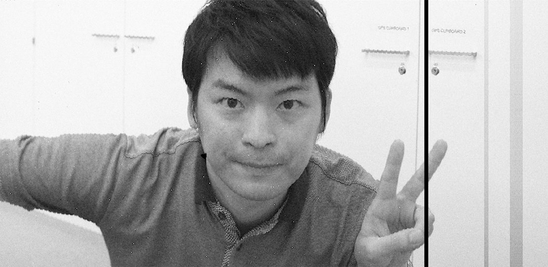
How did you feel when you first got MegaX (the prototype of the million-pixel SPAD sensor) to work?
When we develop image sensors, we consider it a success if we manage to capture an image when the actual chip is mounted to the circuit board. I prepared by doing careful simulations with software. On my first try, I managed to obtain a successful capture from 500,000 pixels out of the 1 million on the SPAD sensor. It was a huge step towards achieving my goal. Even today, I still remember the moment I succeeded in taking a picture of myself in the lab early in the morning when no one was around, flashing a victory sign.
At the same time, the resulting image didn't use all 1 million pixels, so it occurred to me that there could be an issue with the sensor I had designed. After much trial and error, I finally found the source of the problem, which lay in the electrical circuit board. The Mega X prototype was complete only after I fixed that issue.
When I was developing the sensor, I had faith that I would succeed. But when I received the first test sensor, I had only two to three months left in my study abroad program, so I was quite nervous—if it didn't work, the two years I had spent abroad would all be in vain.
We heard that SPAD sensors enable you to see the movement of light.
SPAD sensors can process information within some 100 picoseconds (1/10 billion seconds). This makes them capable of capturing the movement of objects that move extremely quickly, such as light particles. One day, near the end of my time at EPFL, my lab mates and I decided to record an unusual video as proof of working on the same research topic at EPFL, and this is what we took.
(Courtesy of Canon and École Polytechnique Fédérale de Lausanne)
- * In order to view videos, it is necessary to consent to the use of cookies by our website. If the videos are not displayed, please click the "Cookie Settings" and accept cookies.
A light ray can circle around Earth 7.5 times (around 300,000km) in just 1 second. I was amazed that we could capture it in slow motion!
Furthermore, if you observe the video closely, you will notice that the light ray changes speed as it moves. This is a known phenomenon in the astrophysics world, but it usually can be observed only in celestial bodies that are tens of thousands of light years away. I was stunned that we were able to see it happening right there in the lab! It was then that I truly felt the power and potential that SPAD sensors held.
The difficulty of commercialization Not “only a 10% chance” but a chance of “as much as 10%”
After I returned to Japan from Switzerland, I continued R&D on SPAD sensors at Canon. Then after that, through the combined technical expertise and knowhow of various Canon departments, we successfully commercialized the MS-500, an ultra-high-sensitivity interchangeable lens camera that uses a high-resolution SPAD sensor capable of color image capture.
Back before I went to Switzerland to study, when I made the SPAD sensor R&D proposal to my boss, he had told me, “This technology has a 10% chance of being commercialized.”
“Only 10%?” I had asked. His reply to me still leaves a deep impression to this day: “As much as 10%.” That made me realize just how difficult it was for a new technology to reach the commercialization stage—and makes the successful commercialization of the MS-500 feel even sweeter.

The MS-500 is the world's first*1 ultra-high-sensitivity camera equipped with a SPAD sensor for color shooting. It features a 1-inch type SPAD sensor with approximately 3.2 million pixels*2. Capable of capturing clear color images with very little noise even from long distances and in extreme low light environments, it is useful for the surveillance of important infrastructure facilities such as coastlines and power stations, as well as for monitoring purposes such as to prevent river flooding.
- *1 Among color cameras with SPAD sensors. As of July 31, 2023. Based on Canon research.
- *2 Total pixel count: 3.2 million pixels. Effective pixel count: 2.1 million pixels.
Canon developing world-first ultra-high-sensitivity ILC equipped with SPAD sensor
What strengths of Canon did you feel more aware of after returning from EPFL?
I felt that the commercialization of the MS-500, which comes with a unique SPAD sensor, was possible precisely because Canon had extensive industry expertise cultivated over many years. Besides the SPAD sensor, Canon develops its own broadcast lenses and camera image processing engines, so it has many talented people who have a deep understanding of the properties of these products and technologies. These backgrounds are put to good use when those talented people in various departments are encouraged to work together, allowing us to create better products. For example, it enables us to improve the fundamental performance including perceived resolution, gradation and color reproduction, drawing out the best performance of the sensors and lenses.
Next Stage Taking SPAD sensors further: what's next?
I hope to make the SPAD sensor even smaller and increase its pixel count. I am aiming to improve the technology and develop a smaller, higher resolution SPAD sensor to create a smaller, higher resolution camera. By doing so, I want to expand the possibilities of the cameras that Canon makes, improve convenience, and enrich the world.
Last year, Nature named you among the “four rising stars who are reshaping nanoscience”*. You also became the first “Top Scientist” designated under Canon's new HR system for recognizing people with advanced technical expertise.
*From “Four rising stars who are reshaping nanoscience” (August 10, 2022 issue of Nature)
I was honestly surprised to be recognized by Nature, which is one of the top scientific journals in the world. At first, I even thought it was a case of mistaken identity! I'm proud of it, but at the same time, it makes me feel that I have to work even harder. People within the company have high expectations for the technology, too, so there is quite a bit of pressure.
While I learned a lot being able to do research on my own at EPFL, I feel that I'm personally more inclined towards working in a team where everyone shares their opinions as we work on a product. I would like to focus on working on bigger projects that span across other divisions or businesses to produce greater results. Someday, I would like to lead a large team and create technologies and products that will amaze the world.