The semiconductor manufacturing process is broadly divided into chip fabrication and package assembly. Canon’s semiconductor manufacturing equipment supports a wide range of ultra-precise, complex, and diverse processing steps across these stages.
Related Links:
Canon's Lithography Equipment Plays a Key Role in Semiconductor Processing
Semiconductor Chip Manufacturing Process
| Wafer bonding | This technology enables bonding of wafers made from dissimilar materials with different properties at room temperature without load force, and plays a key role in the production of advanced high-performance devices. | 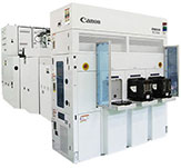 |
|---|---|---|
| Related Links: CANON ANELVA CORPORATION (Atomic Diffusion Bonding Equipment) | ||
| Deposition | This process involves stacking multiple thin films of various materials onto the wafer, which serves as the semiconductor substrate, to control the electrical properties of the semiconductor. | 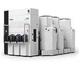 |
| Related Links: CANON ANELVA CORPORATION (Sputtering Equipment) | ||
| Exposure(Front-end) | Light is projected onto a reticle containing a circuit pattern, which is then transferred onto the wafer through projection optics. | 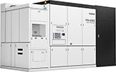 |
| Related Links: Canon Inc.(i-line Steppers, KrF Steppers, Nanoimprint Lithography Equipment) | ||
| Measurement | Wafer distortion is measured, and the data is sent to the lithography equipment for feed-forward alignment correction. | 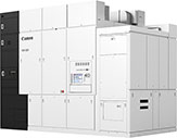 |
| Related Links: Canon Inc. (Wafer Measuring Equipment) | ||
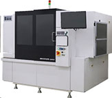
| Die bonding | Diced* semiconductor chips are individually picked and precisely mounted onto lead frames to establish an electrical connection with external wiring. * Dicing: A process in which semiconductor elements are sliced off from the wafer and separated |
 |
| Related Links: Canon Machinery Inc. (Die Bonder) | ||
| Inspection | High-performance three-dimensional measurement is used to automatically inspect each wire, evaluating various features such as wire loop shapes and bonding area geometry. | 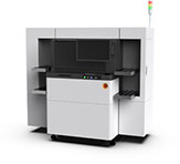 |
| Related Links: Canon Machinery Inc. (Wire Bonding Inspection Equipment) | ||
Package Manufacturing Process
| Deposition | This process rewires various substrates using a highly adhesive film formation method to enable stacking of multiple semiconductor chips and substrates. | 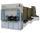 |
|---|---|---|
| Related Links: CANON ANELVA CORPORATION (Sputtering Equipment) | ||
| Exposure(Back-end) | Similar to the front-end process, light is projected onto a reticle containing a circuit pattern, which is then transferred onto the substrate through projection optics. | 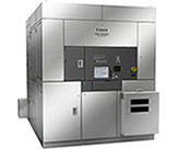 |
| Related Links: Canon Inc. (i-line Steppers) | ||
| Cutting | The IC package substrate, equipped with components such as solder balls, is precisely cut to match the product dimensions. | 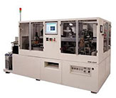 |
| Related Links: Canon Machinery Inc. (Substrate Cutting Equipment) | ||
| Coining | Solder bumps, arranged in high density on the substrate, are precisely flattened by applying pressure with a heated head from above. | 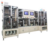 |
| Related Links: Canon Machinery Inc. (Substrate Coining Equipment) | ||
Related Links:
CANON ANELVA CORPORATIONCanon Machinery Inc.