News Release
Canon developing semiconductor lithography equipment employing nanoimprint technology
TOKYO, February 23, 2015—Canon Inc. announced today that the Company is developing a next-generation semiconductor lithography system employing nanoimprint technology that makes possible sub-20 nm1 high-resolution processes.
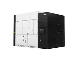
The nanoimprint semiconductor production system
currently under development
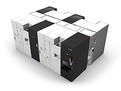
Nanoimprint lithographic cluster system
(conceptual image)
Within the leading-edge high-resolution patterning segment, where 193 nm multiple patterning has become mainstream and EUV (extreme ultraviolet)2 continues to remain in development, in 2004, Canon began conducting research into nanoimprint technology to realize sub-20 nm high-resolution processes. From 2009, targeting the mass production of next-generation semiconductor lithography systems employing nanoimprint technology, the Company has accelerated joint development efforts with Canon Nanotechnologies, Inc., which joined the Canon Group in April 2014, and a major semiconductor manufacturer. Thanks to such technological advances as the development of defect control technologies and improvements in alignment accuracy, Canon is aiming to commercialize a nanoimprint lithography system in 2015.
High-resolution imprint of uniform circuit patterns
In nanoimprint lithography, a mold is brought into direct contact with the resist material on the substrate surface, a pattern transfer process that enables the accurate transfer of the mold's pattern and makes possible higher resolution and more uniform results compared with conventional optical lithographic approaches.3 In addition, unlike optical lithography tools, nanoimprint semiconductor production equipment does not require the use of a light source or high-aperture lens elements, making possible simple configurations and compact designs that enable users to install a cluster of systems for increased productivity.
Lower CoO (Cost of Ownership)4 through greatly reduced production costs
Compared with conventional optical lithography equipment, nanoimprint lithography delivers greatly reduced production costs for semiconductor devices, responding to the high-level demands of semiconductor manufacturers seeking to reduce CoO for high-resolution semiconductor devices. Canon's nanoimprint semiconductor lithography system currently under development will initially target memory device manufacturers producing flash memory. In the future, the Company will aim to apply this technology in the production of DRAM and logic devices.
Canon is planning to present its development progress for the nanoimprint lithography system at the SPIE Advanced Lithography 2015 conference, to be held from February 22 to 26 in San Jose, California, U.S.A.
- 1One nm (nanometer)=one billionth of a meter
- 2EUV lithography is a next-generation lithography technology that uses an extreme ultraviolet wavelength expected to be 13.5 nm.
- 3Semiconductor lithography equipment that employs large-aperture lenses and uses light from a laser to transfer circuit patterns onto a wafer.
- 4Necessary equipment investments and operating costs related to semiconductor production. Used as one of the benchmarks for assessing the productivity of processes and production equipment used in a semiconductor manufacturer's high-volume production line.