News Release
Canon provides nanoimprint lithography manufacturing equipment to Toshiba Memory's Yokkaichi Operations plant
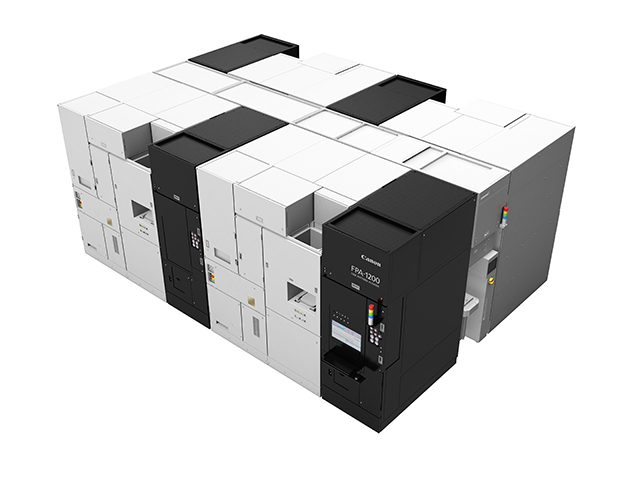
TOKYO, July 20, 2017—Canon Inc. announced today that the company has provided the FPA-1200NZ2C, semiconductor lithography equipment that utilizes nanoimprint lithography (NIL) technology which Canon has been continuously developing since 2004, to leading provider of semiconductor memory solutions Toshiba Memory Corporation's Yokkaichi Operations plant. The provision of this equipment represents significant progress toward semiconductor device mass production that employs nanoimprint technology.

FPA-1200NZ2C
Facing the difficult challenge of circuit scaling, or miniaturization—the key to the advancement of semiconductor devices—Canon has been carrying out R&D since 2004 in the field of next-generation semiconductor manufacturing equipment that utilizes NIL technology which achieves even more detailed circuit patterns as small as 10 nm* at an even lower cost, compared with photolithography†. As part of this effort, Canon welcomed American company Molecular Imprints, Inc. (now Canon Nanotechnologies, Inc.) into the Canon Group in 2014.
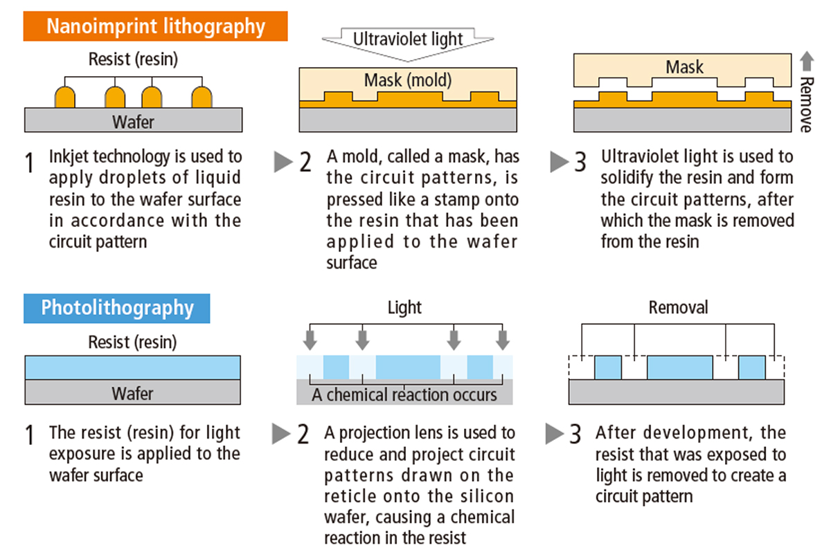
Nanoimprint lithography manufacturing equipment utilizes a patterning technology that involves the field-by-field deposition and exposure of a low viscosity resist deposited by jetting technology onto the substrate, faithfully reproducing patterns with a higher resolution and greater uniformity compared to those produced by photolithography equipment. This technology simplifies the cutting-edge lithography processes used to manufacture semiconductor devices, to make possible a significantly reduced CoO‡ (Cost of Ownership).
Canon's delivery of the FPA-1200NZ2C NIL manufacturing equipment for semiconductor mass production to the Yokkaichi Operations plant of Toshiba Memory further accelerates progress toward the world's first semiconductor memory mass production to utilize NIL technology.
Under the guiding principle of Canon's Excellent Global Corporation Plan Phase V (2016-2020), embracing the challenge of new growth through a grand strategic transformation, the company is positioning its industrial equipment business as one of four new core businesses. Through the practical application of nanoimprint lithography manufacturing equipment, Canon ensures the continued growth of its industrial equipment business.
- *1nm (nanometer) is 1 billionth of a meter.
- †A semiconductor lithography system that utilizes wide-diameter lenses and a light source to transcribe circuit patterns onto wafers.
- ‡Necessary equipment investments and operating costs related to semiconductor production. Used as one of the benchmarks for assessing the productivity of processes and production equipment used in a semiconductor manufacturer's high-volume production line.
About nanoimprint technology
Nanoimprint lithography manufacturing equipment utilizes a patterning technology that involves the field-by-field deposition and exposure of a low viscosity resist deposited by jetting technology onto the substrate. The patterned mask is lowered into the fluid which then quickly flows into the relief patterns in the mask by capillary action. Following this filling step, the resist is crosslinked under UV radiation, and then the mask is removed, leaving a patterned resist on the substrate. The technology faithfully reproduces patterns with a higher resolution and greater uniformity compared to those produced by photolithography equipment. Additionally, as this technology does not require an array of wide-diameter lenses and the expensive light sources necessary for advanced photolithography equipment, NIL equipment achieves a simpler, more compact design, allowing for multiple units to be clustered together for increased productivity.

