News Release
Canon celebrates the 50th anniversary of the PPC-1, Japan's first semiconductor lithography system
TOKYO, January 15, 2020—Canon Inc. today announced the 50th anniversary of the launch in 1970 of the PPC-11, Japan's first semiconductor lithography system, which signaled the company's full-scale entry into the semiconductor lithography equipment business. Semiconductor lithography systems are indispensable for the fabrication of semiconductor devices used in such devices as cameras, smartphones and automobiles. Canon semiconductor lithography equipment has continued to evolve in order to enable the advancement of digital technology.
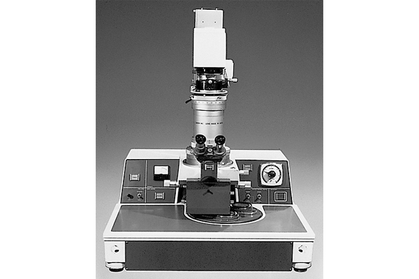
Canon Projection Print Camera (PPC-1)
Japan's first semiconductor equipment
50th anniversary logo
The history of Canon's semiconductor lithography equipment begins with advancements in camera lens technology. Utilizing technology originally developed for camera lenses during the mid-1960's, Canon developed high-resolution lenses for photomask manufacturing. With the aim of expanding its operations, the company began developing semiconductor lithography equipment for wafer fabrication, and in 1970, entered the business with the introduction of the "PPC-1," Japan's first domestically produced semiconductor lithography equipment. Canon later released the FPA-141F in 1975, the world's first lithography system to achieve resolution more precise than 1 micron2 resolution. In 2010, the FPA-141F was recognized by the Center of the History of Japanese Industrial Technology as an Essential Historical Material for Science and Technology.
At present, the Canon semiconductor lithography equipment portfolio includes i-line3 and KrF lithography systems4 to meet an expanding range of applications and market demands. Canon continues to expand its lineup of semiconductor lithography equipment and optional functions with the aim of supporting various wafer sizes and materials and next-generation packaging5 process requirements. Canon also offers leading-edge such lithography solutions as the in-development nanoimprint lithography equipment6 which enables cost-effective circuit pattern miniaturization for mass production processes.
Since 1986, Canon has also leveraged its semiconductor lithography technology in the development, manufacturing and sale of equipment used in the production of flat-panel displays on large-area substrates. Going forward, the company will continue to pursue both higher-resolution and productivity for Canon flat-panel display lithography systems in order to meet the needs of LCD and OLED display manufacturing.
As Canon celebrates the 50th anniversary of its semiconductor lithography equipment, the company will continue to improve and refine its lithography systems with the aim of contributing to the further development of society.
- 1PPC stands for "Projection Print Camera." When released, the PPC-1 was referred to as a semiconductor printing device, not an exposure device.
- 2A semiconductor exposure system using a mercury lamp light source for i-line wavelength (365 nm) exposure. One nanometer (nm) is one-billionth of a meter.
- 3A semiconductor exposure system using laser light generated from krypton (Kr) gas and fluorine (F) gas for KrF wavelength (248 nm) exposure.
- 4The common name for the SI unit micrometer. One micrometer is one-millionth of a meter.
- 5Packaging protects delicate IC chips from the external environment while enabling electrical connection and communication with the external chips and devices.
- 6Nanoimprint lithography involves pressing a mask (mold) directly into the resist on a wafer like a stamp. Circuit patterns including free-form structures on the mask can be precisely transferred with higher resolution in comparison to conventional optical lithography equipment.