News Release
Canon develops SPAD sensor with world-highest 3.2-megapixel count, innovates with low-light imaging camera that realizes high color reproduction even in dark environments
TOKYO, December 15, 2021—Canon Inc. announced today that the company, thanks to a proprietary pixel architecture that efficiently captures and greatly multiplies light, has successfully developed an ultra-small 13.2 mm x 9.9 mm SPAD sensor capable of capturing the world's highest1 resolution of 3.2-megapixel images—a higher resolution than Full HD (approximately 2.07 megapixels), even in low-light environments. Manufacture of the new sensor will commence in the second half of 2022. In addition, a research paper detailing the company's findings has been selected for the Late News Papers2 , an extremely competitive publication of the IEDM3 conference, opened on December 11, 2021.
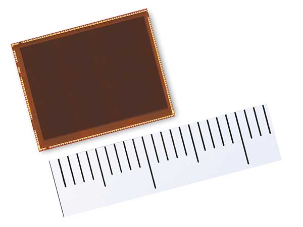
The 13.2 mm × 9.9 mm 3.2 megapixel SPAD sensor
*Size of effective pixel portion shown
A SPAD sensor is a uniquely designed image sensor in which each pixel possesses an electronic element. When a single light particle, called a photon, reaches a pixel it is multiplied—as if creating an "avalanche"—that results in a single large electrical pulse. With CMOS sensors, the readout of the accumulated electronic charge contains electronic noise, which diminishes image quality, due to the process by which accumulated light is measured. Meanwhile, with SPAD sensors, noise does not interfere with the readout of light as electrical signals. This enables clear image capture of subjects that is free from signal noise, and provides such advantages as greater sensitivity during image capture and high-precision distance measurement4.
The newly developed SPAD sensor employs a proprietary pixel architecture that reflects photons inside the pixel in order to effectively detect photons across the entire range of the effective pixels. Under equivalent light, this SPAD sensor can capture the same images as a conventional CMOS sensor while requiring only 1/10 of imaging area. This makes possible an ultra-small design that can be installed even in small devices and greatly increases sensitivity, including for light on the near-infrared spectrum, and realizes video capture with 3.2 megapixels under low-light conditions of 0.002 lux5—darker than a starless night sky. By equipping cameras designed for low-light and monitoring applications with this new SPAD sensor, even video footage of low-light environments can be viewed as if it were recorded in bright areas, enabling identification of subject movement as though viewing with the naked eye in well-lit environments
Beginning in the second half of 2022, Canon will commence manufacturing of SPAD sensors for use in the company's security-oriented network camera products. With the inclusion of this innovative sensor, Canon's products will gain a competitive edge and contribute to the realization of a more safe and secure society.
In addition, the SPAD sensor is capable of extremely high information processing speeds on the level of 100 ps (picoseconds, one-trillionth of a second), enabling it to capture objects moving at high speeds including photons. With a resolution that surpasses Full HD and high sensitivity that enables capture of faint light, the sensor's unique rapid response functionality can be utilized in a wide range of applications including self-driving vehicles, medical treatment, diagnostic imaging devices and scientific precision measuring instruments. Canon will proactively expand its sales network in order to encourage further innovation and development of society.
- 1Among SPAD sensors. As of December 14, 2021. Based on Canon research.
- 2An extremely competitive selection of research papers submitted to the IEDM (see footnote 3).
- 3International Electron Devices Meeting, the leading international conference for the field of semiconductors.
- 4For more information on the differences between SPAD and CMOS sensors, please visit Canon's Technology Website at: https://global.canon/en/technology/spad-sensor-2021.html
- 5Light from stars estimated at 0.02 lux. Ambient light in starless night environment estimated at 0.007 lux.
Example applications for SPAD sensors
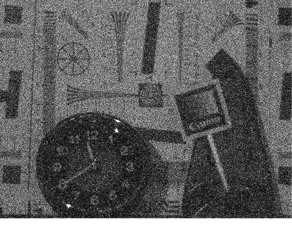
This SPAD sensor was installed in a prototype camera* which was used to capture video with a exposure rate of 1/30 seconds. The three images below are still images extracted from the captured video.
Using the SPAD sensor, researchers successfully captured color images in an indoor environment at a resolution of 3.2 megapixels (greater than Full HD) (a). Under conditions of 0.002 lux, darker than a starless night environment (approximately 0.007 lux), researchers were able to obtain clear monochrome intensity images of background resolution testing patterns, as well as moving objects such as a metronome needle or the second-hand needle of a clock (b-1). Furthermore, images, in which subjects could be identified, were obtained in a specially created darkroom with low-light conditions of 0.0003 lux, in which the naked eye cannot discern surrounding objects (b-2).

(a) Indoor scene

(b-1) 0.002 lux
*Darker than starless night conditions
(b-2) 0.0003 lux
*Equivalent to conditions in which naked eye cannot perceive objects
- *Lens used: Canon EF50mm f/1.2L USM (released in January 2007). Image (a): RGB color filter used. Image (b): no color filter used. Both images (a) and (b) were not subjected to post-processing.
Architecture and characteristics of the SPAD sensor
In conventional backlit SPAD sensors, only photons within the space covered by an electrical field (sensitivity field) can be detected, creating a challenge requiring pixel size to be shrunk and as a result, sensitivity to be lowered. With the proprietary voltage accumulation architecture of this new SPAD sensor, the space within the sensitivity field covers the entire pixel area, increasing the amount of photons that reach the light-receiving pixels. This makes possible a photon use efficiency of 100%, including within the near-infrared range, with a pixel pitch of 6.39 μm, realizing both miniaturization and high sensitivity. As a result, clear images with the world's highest resolution of 3.2 megapixels can be captured under environments equivalent to starless night skies as dark as 0.002 lux.
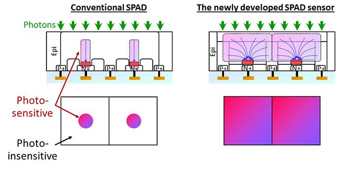
Fig. 1. Cross-sectional views and top-view layouts of conventional BSI SPAD array (left) and BSI charge focusing SPAD array (right).
In addition, thanks to a proprietary voltage accumulation architecture that increases photon collection efficiency, the sensor achieves exceptional performance in three different metrics: (1) near-infrared light spectrum sensitivity, (2) low noise and (3) high detection speed (temporal resolution).
(1) Near-infrared spectrum sensitivity
Increased PDE (Photon Detection Efficiency), or the ability to capture more light, enables this SPAD sensor to capture a wider range of light—from the visible spectrum to the near-infrared* spectrum—a significant increase compared to previous Canon-developed SPAD sensors. Capitalizing on the ability of near-infrared light to pass through objects, this makes possible such applications as monitoring and measuring under fog or other poor-visibility conditions, as well as the detection of foreign objects during industrial inspection processes.
- *A type of electromagnetic wave with a wavelength near that of the red portion (700 – 2500 nm) of the visible light spectrum. While not visible to the human eye, near-infrared light possesses properties close to those of visible light. For this reason, it is known as "invisible light" and is used in a variety of technologies including remote controls for household electronic appliances and infrared signal transmission devices.
(2) Low noise
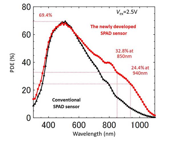
Lower levels of noise corresponds to a lower DCR (Dark Count Rate). When attempting to lower this value, there is generally a resulting trend towards lower PDE. This new SPAD sensor, however, lowers DCR while achieving a PDE of 69.4%.
(3) High-speed detection (temporal resolution) and high-sensitivity
When decreasing temporal resolution—the time required to detect photons—there is a corresponding trend indicating a drop in PDE. This new SPAD sensor, however, achieves a high PDE of 24.4% for 940 nm wavelength light on the near-infrared spectrum with a time resolution of 100 picoseconds (one ten-billionth of a second).
(1) Measured PDE comparison between previous Canon-developed SPAD sensors and the newly developed SPAD sensors
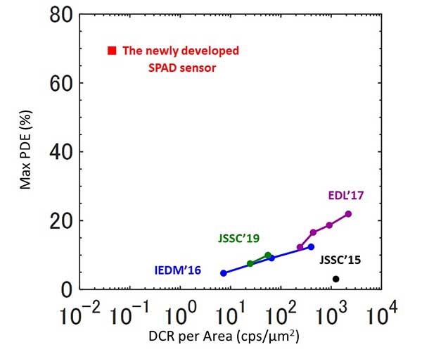
(2) Max PDE versus
DCR per unit photo-sensitive area
(Vex=2.5V)
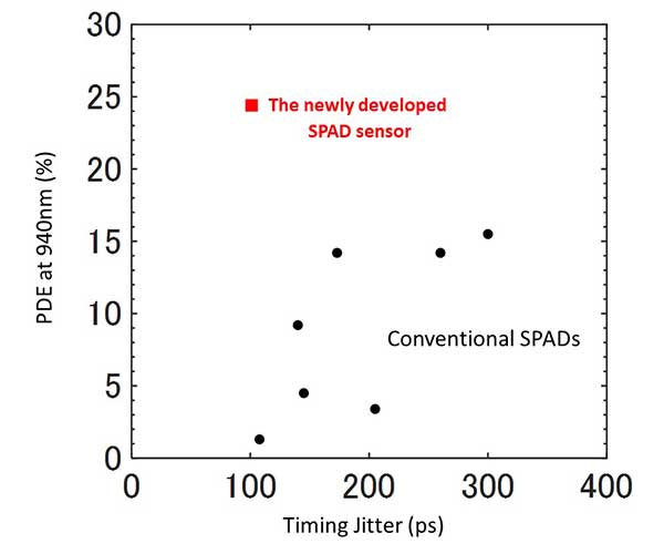
(3) Comparison of temporal resolution (time jitter) and PDE
(Vex = 2.5V)
These characteristics help make possible image capture in dark environments with similar results as if captured in bright, well-lit environments, making the sensor ideal for devices such as security-oriented network cameras for monitoring dark outdoor environments or extremely dark automated manufacturing facilities, as well as cameras for ecological research in low-light conditions.
In addition, thanks to temporal resolution and high sensitivity that enables the capture of light trajectories moving at speeds of approximately 300,000 km/s (equivalent to 7.5gs), there are expectations that this technology may be used in the process of obtaining high-speed, high-precision 3D special information for such applications as distance measurement for automated vehicles, Augmented Reality (AR) and Mixed Reality (MR). What's more, in the field of medicine, this sensor holds the potential for use in camera components of medical diagnostic imaging devices, microscopes and other equipment. Such devices may be used to determine the behavior and position of fluorescent substances in patient bodies that emit faint light in extremely brief time spans, thereby potentially helping to identify early-stage cancer cells or other illnesses or localized afflictions in their initial stages.