Canon Science Lab
CCD Sensors
CCD stands for "charge coupled device," a semiconductor image sensor used in digital cameras to convert light into electrical signals.
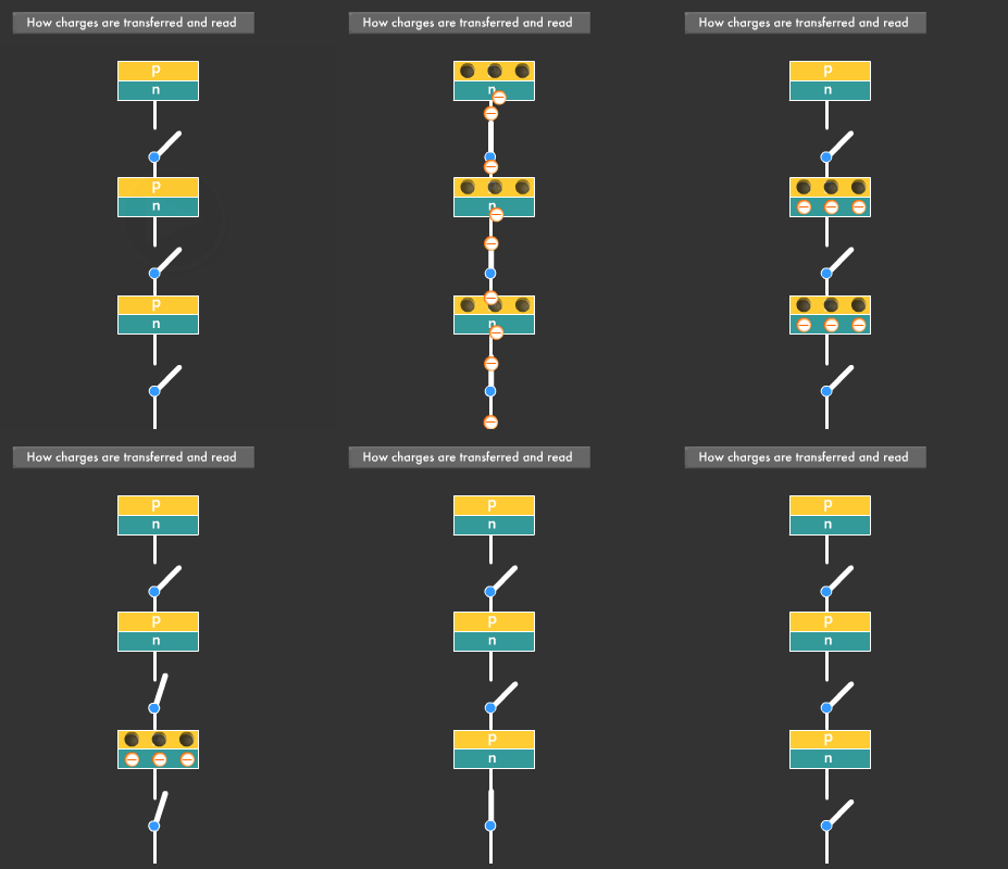
In place of the film used in conventional film cameras, digital cameras incorporate an electronic component known as an image sensor. Most digital cameras are equipped with the image sensor known as a CCD Sensors, a semiconductor sensor that converts light into electrical signals. CCD Sensors are made up of tiny elements known as pixels. Expressions such as "2-megapixel" and "4-megapixel" refer to the number of pixels comprising the CCD Sensors of a camera. Each pixel is in fact a tiny photodiode that is sensitive to light and becomes electrically charged in accordance with the strength of light that strikes it. These electrical charges are relayed much like buckets of water in a bucket line, to eventually be converted into electrical signals.
The Way Light Is Converted Into Electric Current
The surface of a CCD Sensors is packed with photodiodes, each of which senses light and accumulates electrical charge in accordance with the strength of light that strikes it. Let's take a look at what happens in each photodiode. Photodiodes are, in fact, semiconductors, the most basic of which is a pn pair made up of a p-type and an n-type semiconductor. If a plus electrode (anode) is attached to the p-type side, and a minus electrode (cathode) is attached to the n-type side of the pn pair, and electric current is then passed through this circuit, current flows through the semiconductor.

This is known as forward bias. If you create a reversed circuit by attaching a plus electrode to the n-type side, and a minus electrode to the p-type side of the pn pair, then electrical current will be unable to flow. This is known as reverse bias. Photodiodes possess this reverse bias structure. The main difference from standard semiconductors is the way in which they accumulate electrical charge in direct proportion to the amount of light that strikes them.
Photodiodes Accumulate Electrical Charge
Photodiodes are designed to enable light to strike them on their p-type sides. When light strikes this side, electrons and holes are created within the semiconductor in a photoelectric effect. Light of a short wavelength that strikes the photodiode is absorbed by the p-type layer, and the electrons created as a result are attracted to the n-type layer. Light of a long wavelength reaches the n-type layer, and the holes created as a result in the n-type layer are attracted to the p-type layer. In short, holes gather on the p-type side, which accumulates positive charge, while electrons gather on the n-type side, which accumulates negative charge. And because the circuit is reverse-biased, the electrical charges generated are unable to flow.

The brighter the light that hits the photodiode, the greater the electrical charge that will accumulate within it. This accumulation of electrical charge at the junction of the pn pair when light strikes is known as a photovoltaic effect. Photodiodes are basically devices that make use of such photovoltaic effects to convert light into electrical charge, which accumulates in direct proportion to the strength of the light striking them. Photodiodes are also at work in our everyday lives in such devices as infrared remote control sensors and camera exposure meters.
CCD Sensors Relay Electrical Charge Like Buckets of Water in a Bucket Line
CCD Sensors comprise photodiodes and mechanisms consisting of polysilicon gates for transferring the charges accumulating within them to the edge of the CCD. The charges themselves cannot be read as electrical signals, and need to be transferred across the CCD Sensors to the edge, where they are converted into voltage. By applying series of pulses, the charges accumulated at each photodiode are relayed in succession, much like buckets of water in a bucket line, down the rows of photodiodes to the edge. CCD is the abbreviation of "Charge-Coupled Device," and "Charge-Coupled" means the way charges are moved through gates from one photodiode to the next.

