Canon Science Lab
Semiconductor Lithography Equipment
Semiconductor lithography equipment are used to project electrical circuit patterns on silicon wafers Capable of etching extremely detailed patterns on the scale of nanometers (1 nm = one billionth of a meter) these devices use ultrahigh-precision optical and engineering technologies.
Electrical components such as computer microprocessors and memory chips contain nanometer-level electrical circuits that have been patterned using a semiconductor lithography equipment. A laser beam is shone on a "photomask," or an original circuit pattern, to create an image of the circuit on a silicon wafer. Creating such nanometer-level circuitry requires ultrahigh-precision lenses and wafer stages, which are used to carry the silicon wafers that serve as the foundations for semiconductor devices. Semiconductor lithography equipment have played a key role in the remarkable advances made in semiconductor circuit integration in recent years.
Using Laser Light to Create Circuits
Semiconductor lithography equipment project a reduced image of the photomask, the original circuit pattern, onto the silicon wafer, which is coated in a photosensitive layer called a photoresist. Projecting the circuit pattern onto the photoresist leaves an image of the circuit on the photoresist in much the same way that illuminating light through a film negative leaves a latent image on photo printing paper. After exposure, the wafer is subjected to developing, etching, doping and other processes that leave just the circuit on the wafer.
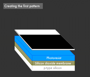
Developing involves the immersion of the wafers in developer to dissolve and remove unexposed, unnecessary photoresist, while etching removes the surface membrane of silicon dioxide through a chemical reaction, and doping adds conductive impurities through ion irradiation. This series of processes is repeated over 30 times to complete a single IC chip. The diagram below shows the steps involved in manufacturing a simple transistor.
The Completed Semiconductor
In the completed transistor, n-type silicon has been embedded in p-type silicon by doping, after which the non-conductor (isolator) and conductor are incorporated. If electric current runs through this circuit, electrons gather through electrostatic induction in the area of the p-type silicon opposite the conductor, enabling current to pass between the n-type silicon points. The way in which the p-type silicon is affected by the electric field of the conductor, despite its being isolated by the non-conductor, is referred to as field effect. This transistor works by switching the current on and off.

This kind of transistor, in which a non-conductor (isolator) and metal conductor are placed on top of a semiconductor, is known as an MOS (Metal Oxide Semiconductor), and an MOS that makes use of field effect is further known as an MOS FET.
Ultrahigh-precision Wafer Stage Positioning Technology
The precision with which the wafer stage, which carries the silicon wafers, is positioned is of critical importance in semiconductor lithography equipment, since the wafer must be moved at high speed but very accurately during the exposure process. Etching a 130 nanometer-wide circuit requires an error factor of not more than (10 nanometers. To attain such precision, the wafer stages of Canon's semiconductor lithography equipment employ a non-contact air guidance system that uses porous ceramic static pressure bearings and a linear motor, with the wafer stage being pneumatically floated. This eliminates friction, and enables high-speed, accurate positioning. This wafer stage can control wafer position in all three dimensions to within a few nanometers. In the future, circuits will be even further miniaturized, and wafer stages offering sub-nanometer precision will be required. Semiconductor lithography equipment of the future will likely require a vacuum to boost circuit patterning precision further, and Canon is currently working on the development of vacuum air bearings technology to enable the use of air bearings in a vacuum.
Next-generation Semiconductor Lithography Technology
Because photolithographic optical apparati project very detailed circuit patterns onto wafers, they need to use very short wavelength light sources. Current devices use 248 nm KrF (krypton fluoride) or 193 nm ArF (argon fluoride) excimer lasers as light sources, which are capable of creating circuit patterns of a width of about 100 nanometers. Various other light sources are currently being studied to get this size down to the 50 nanometers that will be required in the future. In addition to fluoride dimer excimer lasers with wavelengths of 157 nm and X-ray lasers, EUV (Extreme Ultra-Violet) light sources are attracting keen attention.
EUV sources have wavelengths of just 13 nanometers, and so should be well able to create patterns of under 50 nanometers. However, because almost all materials absorb EUV, refractive optical elements cannot be used to control the EUV path, and special mirrors, known as multilayer coating mirrors because their surfaces are coated with multilayer thin-film coatings, are being developed. The coatings consist of a large number of alternating layers of materials having slightly different refractive indices to provide a resonant reflectivity to EUV. The manufacture of multilayer reflectors, in turn, requires very high precision coating technologies to deposit coatings with atomic-level thicknesses.
Mirror Projection Aligners for Exposing Large Liquid Crystal Panels
Exposure technology is also used in the manufacture of large liquid crystal panels — the exact opposite of small silicon chips — such as those used to create large LCD televisions. Liquid crystal panels are manufactured by projecting a detailed pixel pattern drawn on an optical mask to etch (expose) and develop a large glass substrate. Mirrors and lenses are used in the projection process, but reflective optical systems using mirrors have a simpler composition than transparent optical systems using lenses, providing such benefits as no chromatic aberration and no deterioration in imaging performance.
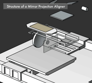
In order to expose patterns measuring just several micrometers in size, the mirrors used in mirror projection aligners must be extremely precise. Specifically, large-diameter concave mirrors able to ensure the exposure width and scan distance required for seamlessly exposing large screens with a single pass. Furthermore, due to the size of the glass substrates used, with some measuring as large as 2,200 x 2,500 mm ("8th generation" substrates), an ultra-large stage that moves with precision is also required.