Technology that transcends human vision The Story Behind the Development of Canon's Most Advanced CMOS Sensor
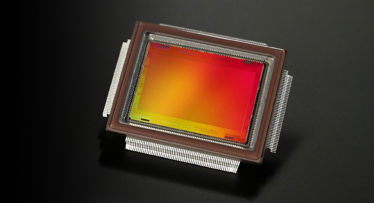
The CMOS sensor is the very heart of the camera, and Canon has long pursued in-house development and production of these devices. Working together as a dedicated team, Canon's engineers have succeeded in developing the industry's most advanced CMOS sensor. This revolutionary technology is expected to spark wide-ranging innovation as the leading image sensor in the age of the "Internet of things," or IoT, which is expected to greatly expand the market scale for CMOS sensors.
Introducing Canon CMOS sensor technology
*In order to view videos, it is necessary to consent to the use of cookies by our website. If the videos are not displayed, please click the "Cookie Settings" and accept cookies.
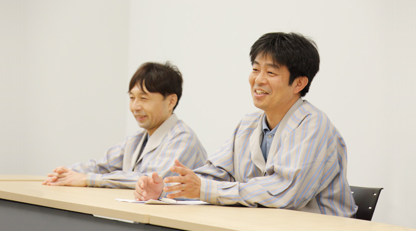
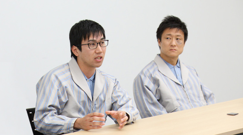
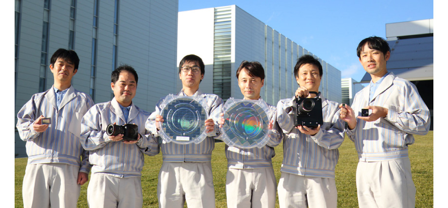
Developers interviewed
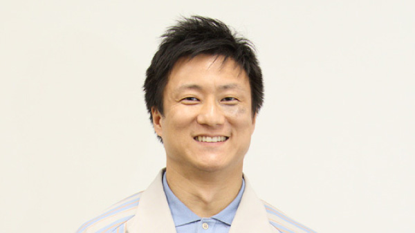
Tatsuya Ryoki
- In charge of device design
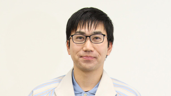
Keita Torii
- In charge of process development
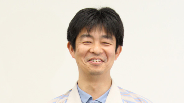
Hiroo Akabori
- In charge of device design
Shigeru Kido
- In charge of semiconductor manufacturing technology
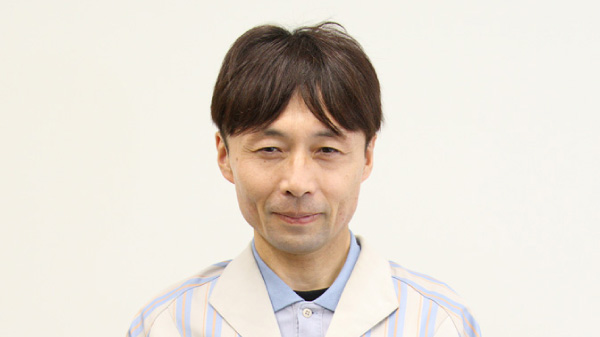
Yusuke Onuki
- In charge of device element development
Kenji Takata
- In charge of device sales promotion
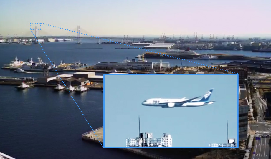

Imagine being able to read the lettering on the side of an airplane 18 km away!
A sensor incorporating an extraordinary 250 million pixels
In 2010, Canon attracted considerable attention for introducing a 120-million-pixel CMOS sensor. The next mission assigned to the development team was to design an image sensor with an extraordinary 250 million pixels. How did they overcome the daunting challenge of miniaturizing the pixels and increasing the processing speed of peripheral circuits?
Tatsuya Ryoki
In charge of device design
Mr. Ryoki joined the company in 2004, gaining experience in the Semiconductor Material Development Department. Since 2007, he has been responsible for sensor development. He takes a proactive approach to tackling technical challenges: instead of getting caught up in "why not" or "why can't," he focuses on "how can" problems can be solved.
This 250-million-pixel sensor is capable of rendering the characters on the side of an airplane 18 km away. What was the inspiration for the development of this CMOS sensor?
Tatsuya Ryoki
By 2010, Canon had already developed a 120-million-pixel CMOS sensor, a number equivalent to the amount of photoreceptor cells in the human eye. So, we undertook the challenging task of developing a 250-megapixel image sensor as a means of demonstrating the overwhelmingly superior acuity of Canon's sensor, which in this case is twice that of human vision.
Kenji Takata
Even if we were to successfully increased the number of megapixels to 130 or 140, our competitors would soon catch up to us. So instead, we decided to aim for double the number of pixels right off the bat. [Laughs]
Ryoki
But instead of simply increasing the number of pixels, we also became very particular about the actual performance of each pixel in order to ensure the captured image was appealing. Despite the many difficulties involved, we succeeded in realizing the levels of performance we were after.
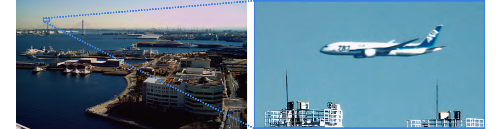 The captured image (left) is achieved using a digital zoom, and image-processing technology is then applied (right). As a result, the letters on the side of the aircraft about 18 km away become legible, a feat beyond the ability of the human eye alone. (Captured with a prototype camera, equipped with an EF800-mm telephoto zoom lens with digital zoom applied.)
How difficult a goal was 250 million pixels?
Ryoki
Remember that all the components must be packaged in a sensor chip of limited size. To make this happen, the close cooperation of the three divisions involved was essential—that is, the Device Design Department, in charge of developing the CMOS sensor pixel structure, the Process Development Department, in charge of developing the manufacturing processes, and of course the production plant itself.
Keita Torii
In charge of process development
Since joining the company in 2008, Mr. Torii has been responsible for developing the technology used to manufacture CMOS sensors. He makes a concerted effort to expand the scope of his field and abilities, even with subjects that are outside his area of expertise.
Keita Torii
In general, the process development focused on two major issues. One was the miniaturization of pixels, because twice the number of pixels found in a conventional sensor had to be integrated into a chip of the same area. The other issue was ensuring that these miniaturized pixels receive adequate light.
Shigeru Kido
The pixels in a CMOS sensor comprise many semiconductors. So, these pixels must be manufactured uniformly in order to make sure that received light is directed to all pixels evenly. It's a much greater challenge to meet the required levels of miniaturization and uniformity than it is for other semiconductor devices like memory. As you can imagine, increasing the yield of the plant production processes is quite a challenge.
Torii
For example, the conventional standard for judging a defective product is contamination with dust at the 1-micron level. But given the level of miniaturization involved with this device, intrusion of a dust particle measuring as small as 0.1 microns can result in a defective product.
As you approached the 250 megapixel level, wasn't it also necessary to double the Sensor's data-handling capacity?
Ryoki
To capture 5 frames per second, you need a signal-processing capacity of 1,250 megapixels per second. So, as you might expect, the peripheral circuitry must be capable of such high-speed data processing. A CMOS sensor actually handles two processes—the electronic circuit-forming process and the pixel-forming process. Reconciling these two processes presented us with quite a challenge.
What made it so challenging?
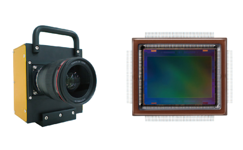 Prototype camera (left) equipped with a 250-megapixel CMOS sensor (right)
(Shown with EF35 mm f/1.4L USM)
Ryoki
As for the circuitry, the peripheral circuits are designed to process at a higher speed and lower voltage than is typical with a conventional device. Applying the same operating conditions to the pixel processes, however, can have an adverse effect on pixel characteristics. At the initial stage of development, we designed the chip with new processes for high-speed circuits, but we were unable to achieve the intended pixel characteristics. For example, when we shot a black test screen, numerous white flaws appeared.
To identify the cause of these flaws, we actually split the chip in half to study it in cross-section. In doing so, we learned that the temperature applied in the peripheral circuit processes was insufficient for the pixel processes.
Yusuke Onuki
As a result of this finding, the team responsible for pixels conducted a simulation to determine the ideal conditions for compatibility between the peripheral circuit processes and the pixel processes. Based on the outcome, we offered suggestions to the circuit design team and the process team.
Torii
Being able to work in such close collaboration with the design, product and factory teams was a significant advantage when overcoming challenges.

Seeing clear as day in pitch-black darkness
An ultra-high-sensitivity sensor with unmatched capabilities
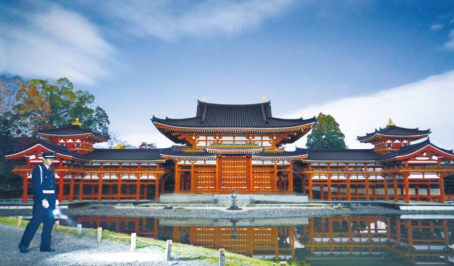
A Canon advertisement appeared in Japanese newspapers on New Year's Day 2017, featuring a photo of the Phoenix Hall in Kyoto's Byodoin Temple. While the colors depicted were especially vivid, there was another aspect of this photo worth noting: it was actually taken at midnight.
How did Canon's engineers manage to create a sensor of such ultra-high sensitivity that it can capture an image at midnight yet make it seem as if it were taken in broad daylight?
Hiroo Akabori
In charge of device design
After joining the company in 1995, Mr. Akabori was put in charge of circuit design, evaluation and production technology. He aims to develop better products by communicating with related departments to deepen his understanding of a wide spectrum of technologies.
The photograph of Byodoin Temple's Phoenix Hall is no ordinary landscape photo, as it was actually shot at midnight. Clearly, the performance of this sensor is nothing less than astonishing.
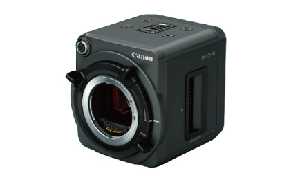 The ME20F-SH, Canon's first ultra-high-sensitivity multi-purpose camera
Hiroo Akabori
In 2013, Canon developed a full-size 35-mm ultra-high-sensitivity CMOS sensor specifically tailored to capture video. This sensor can capture video in a dark room lit by nothing but a single incense stick. In other words, only 0.05 to 0.01 lux of illuminance is required.
In 2015, in pursuit of more advanced low-light performance, Canon developed a sensor capable of capturing color video at illuminance levels of 0.0005 lux or less. Canon then introduced a camera incorporating this sensor, the ME20F-SH—the first multi-purpose camera to feature such ultra-high sensitivity. It was this camera that captured the photo of Byodoin Temple's Phoenix Hall, the photo used in the newspaper ad.
Compared to commercially available digital SLR cameras, this camera achieves exceptionally high sensitivity.
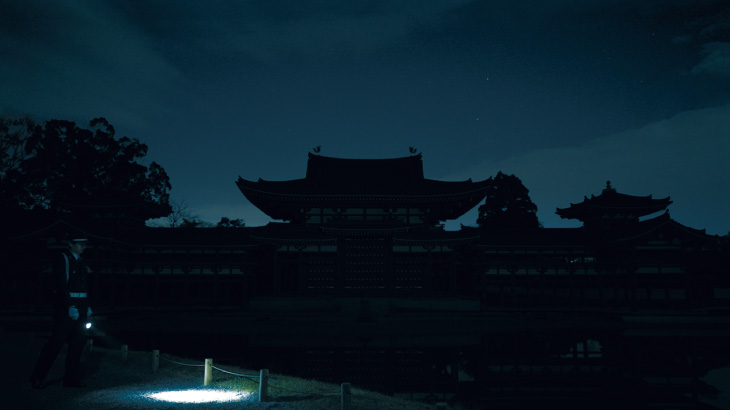 Photo of Phoenix Hall at Byodoin Temple, captured at midnight
(Click on the button above to see the difference.)
Photo of Phoenix Hall at Byodoin Temple, captured at midnight
(Click on the button above to see the difference.)
Akabori
For comparison, it has pixels that are 7.5 times larger than those in the sensor found in Canon's flagship EOS-1D X Mark II. Such cameras generally have a maximum ISO sensitivity of about 3,200. However, a camera with the ultra-high-sensitivity CMOS sensor realizes an ISO sensitivity of 4 million.
Conventionally, our company develops sensors to meet specifications stipulated by the Business Department. However, we now intend to consider our own technical roadmap and proactively suggest new image sensor designs to the Business Department. This ultra-high-sensitivity CMOS sensor was the first step towards that.
But from a marketing perspective, it's not that impressive to emphasize technical superiority in terms of an "ISO sensitivity of x." So instead, we pursued development of this sensor under the slogan, "ISO sensitivity that surpasses even a high-end digital SLR," to emphasize the technical advantages while corresponding to our own technology and needs.
How did you design the sensor to provide higher sensitivity?
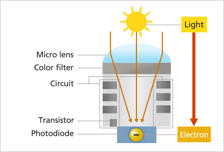 Internal structure of one pixel
Akabori
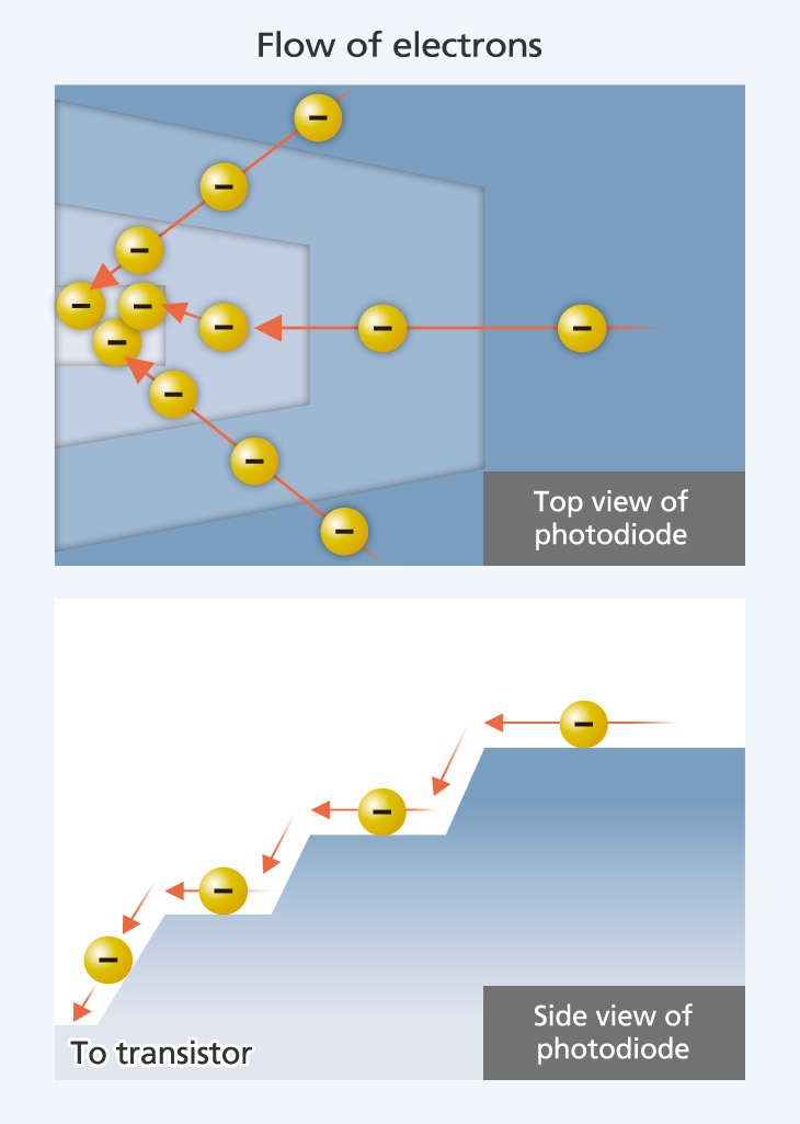
To get an idea of the internal structure of the pixels in a CMOS sensor, imagine that light reaches each pixel, the maximum amount of light is captured via the micro lens, and is then directed to the light-detecting photodiode.
To achieve high sensitivity, you need to enlarge each pixel so it can receive more light. Like I explained before, we adopted a pixel size at least 7.5 times larger than that of a conventional SLR camera. Naturally, this presented difficulties in terms of designing a large micro lens and adapting mass-production technology. It also introduced the problem of a long information read time due to the increased area involved.
 Multi-stage potential structure used in the photodiode
Basically, "information reading" is a process in which electrons converted from light via the photodiode are transferred to the reading circuit through a transistor. Eventually, we came up with a way to shorten read time. We hit on the idea of applying technology we developed for our huge CMOS sensors used in astronomical observation, designing a multi-stage potential structure within the pixels to facilitate the flow of electrons. However, considering the number of stages and their shapes and angles, etc., such a slope structure could be configured tens of thousands of ways. Through an enormous number of simulations, we were able to optimize this structure in order to enable efficient information reading even with such a large pixel size.
Shigeru Kido
In charge of semiconductor manufacturing technology
Since joining the company in 1996, Mr. Kido has been involved in such projects as process development for semiconductor manufacturing equipment and yield improvement of mass-produced CMOS sensors. His motto is taken from the words of Akira Ogi, former manager of the Orix Buffaloes pro baseball team: "Perseverance and hard work open a clear path forward."
Kido
Since the signal level of the ultra-high-sensitivity sensor is higher than that of other sensors, contamination by even minute dust or metal particles can have a significant negative impact. In a mass-production plant, you've got to completely eliminate this risk.
Tackling new challenges requires continued trial-and-error for design, processes and manufacturing. Throughout this project, the developers involved collaborated closely while repeatedly conducting experiments to find solutions.


A change in perspective leads to a newly developed global shutter
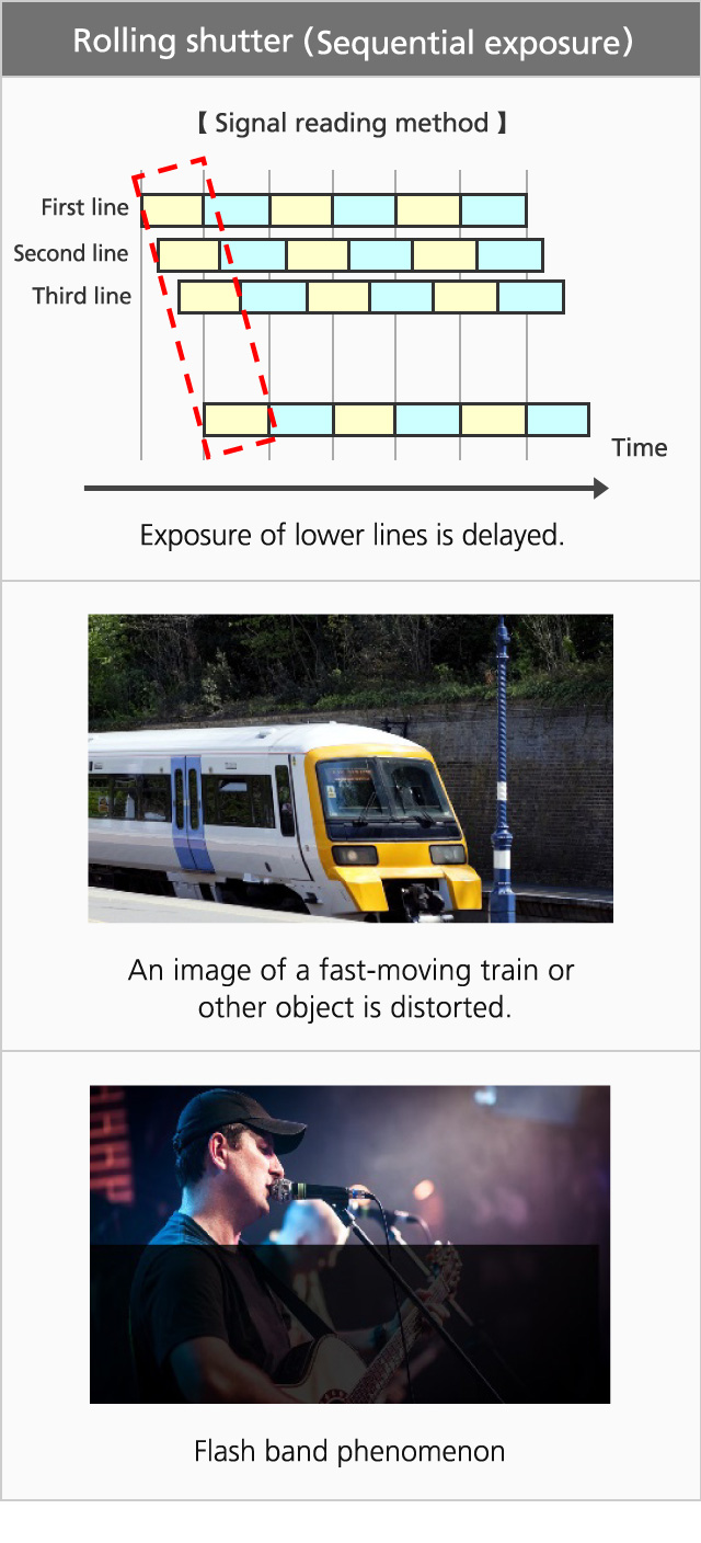
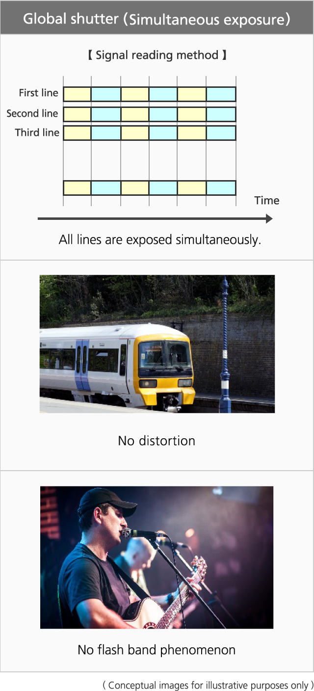
In general, when a conventional CMOS sensor is used to shoot a fast-moving object such as a train, the target image is sometimes distorted. Adding a global shutter to a CMOS sensor can prevent this phenomenon. However, a number of difficulties were encountered in the development of this CMOS sensor. What compelled the developers to change their viewpoint and come up with a global shutter while also achieving a wide dynamic range?
Yusuke Onuki
In charge of device element development
Mr. Onuki joined the company in 2007. He is responsible for CMOS sensor pixel development and process integration. He tends to consider things from multiple angles, aiming to develop products with international appeal.
You developed a CMOS sensor equipped with a "global shutter." But what exactly is a global shutter?
Onuki
When an image is recorded with a digital camera or video camera, the intensity of light that hits the CMOS sensor pixels determines the number of electrons that accumulate. The image data is obtained by reading these electrons.
Conventional CMOS sensors use the rolling shutter method, which performs pixel exposure and reading of electrons line by line. As a result, there is a time lag between the exposure of the first line and exposure of the last line. So, when shooting a moving object such as a train or a rotating propeller, the captured image can be distorted. What's more, if a flash is used during shooting, a difference in brightness can appear between the upper and lower parts of the captured image, something known as the "flash band phenomenon."
I see. I've seen distorted images of trains. I suppose that's what caused the distortion.
Onuki
Yes, but with a global shutter, all pixels are exposed to light at the same moment. This eliminates that distortion as well as the flash band phenomenon.
How did you manage to achieve this global shutter?
Onuki
Imagine that each pixel in the CMOS sensor is like a bucket. With the rolling shutter method, the CMOS sensor has one bucket, that is, the photodiode that receives the light. The electrons are sequentially read from this.
A CMOS sensor using the global shutter method, on the other hand, has two buckets: one is the photodiode, and the other is memory that temporarily stores electrons from the photodiode. With the global shutter, all electrons from the photodiode bucket are sent into the memory bucket at precisely the same moment.
However, this method poses a significant problem.
And what is that?
Onuki
When a pixel is provided with two buckets — the photodiode and memory — the size of each bucket is reduced.
For example, a 10-liter bucket can express anything from empty status to 10-liter full status. But with a 5-liter bucket, the scope of expression is less than what would be available with a 10-liter bucket.
One of the most important performance indices of an image sensor is its dynamic range. Dynamic range indicates the ratio of a signal's minimum value to its maximum value. Put simply, think of it as the size of the bucket. As the dynamic range increases (with a larger bucket), the sensor is capable of expressing a wider range in terms of brightness and color.
So, how did we achieve both a global shutter and dynamic range? To solve this problem, we developed a new drive method.
We did consider developing a global shutter that uses the standard method where the buckets of the photodiode and memory were the same size. However, with this new drive method, we were able to devise creative solutions for the photodiode and memory bucket sizes and the transmission method.
How did you implement this idea?
Onuki
Team members—selected regardless of their professional background—discussed how to achieve both a global shutter and dynamic range. Assembling members from different backgrounds sometimes results in disagreements, however, we encouraged all members to voice their opinions without hesitation and to share ideas from different viewpoints. We adopted their suggestions and conducted repeated trial-and-error with prototype models. The new drive method was derived from one of these prototype models.
Of course we didn't pull the idea for the new drive method out of thin air. Everyone was working hard trying to think of solutions, and from there this technology was born.

Collaborative design, development and manufacturing gives rise to a next-generation sensor
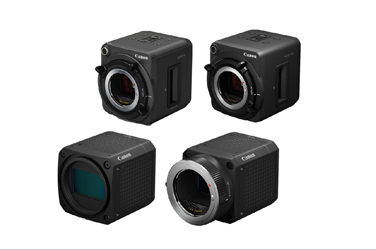
The growing automotive and industrial machinery sectors are driving the rapidly increasing demand for image sensors. How quickly can the sensors demanded by industry be developed and introduced onto the market? As these sensors target industries that differ substantially from the consumer market, developers are facing numerous challenges.
Kenji Takata
In charge of device sales promotion
Mr. Takata joined the company in 2003 and participated in the development of OLED displays. He is now in charge of sales promotion of CMOS sensors. His goal is to help people by establishing a device business that contributes to a safer, more secure and more convenient society.
To date, Canon has used its proprietary sensors for the in-house manufacture of its digital cameras. Now, however, Canon is positioning its image sensors for external sales.
Takata
Canon established a sales promotion project in January 2015 to meet the challenge of distributing its products for external sales. Sensors featuring ultra-high pixel counts and ultra-high sensitivity are very good at emphasizing Canon's technological strengths, but target relatively niche markets.
On the other hand, a CMOS sensor equipped with a global shutter is a key product that is expected to become a mainstream feature of industrial cameras going forward.
What do you mean?
Takata
In the U.S.A., as well as in Japan, there has been an ongoing trend toward "reshoring" the manufacturing sector. However, to pursue manufacturing in developed countries with high labor costs, reducing costs through automation is essential. For that reason, demand for industrial cameras that can perform such tasks as automated product inspection is expected to grow.
Apart from industrial applications, demand for automotive uses is also increasing. The UN World Forum for Harmonization of Vehicle Regulations is prescribing international standards for automobiles. They stipulate that, as of June 2017, combined camera-and-monitor systems will be mandated as substitutes for side mirrors as an international standard. Also, automatic emergency braking systems will be considered compulsory. Image sensors play important roles in these applications.
Is there a difference in product planning between consumer-level and industrial-use products?
Takata
Consumer-level cameras are intended for use by people, while automotive cameras are designed to be incorporated in machines. Industrial machinery must be able to run for 24 hours a day, 365 days a year without breaking down. Also, automobiles are required to function normally even in harsh environments, in both hot and freezing weather.
Canon's image sensors are considered industry leaders in terms of image quality. But as we go forward, it will become increasingly important to exhibit superiority in terms of durability and environmental resistance, as well as image quality.
Onuki
Conventionally, image sensors have been used to record images captured by the human eye. From now on, image sensors will be used in applications that exceed the ability of the human eye. Image sensors will play an active role in new sensing applications by, for example, capturing objects in extreme darkness or brightness, and capturing objects moving at ultra-high speed.
It seems the roles played by image sensors are change significantly. Who do you think should be involved in developing such new products? What type of people do you prefer to work with?
Takata
I think it's important for developers to work with the global market in mind, and aspire to become industry leaders.
Kido
As mentioned before, there is a difference in the specifications required of image sensors for consumer use and those for industrial applications. So, developers must be able to cope with change and be willing to take on challenges in new fields.
Akabori
Product development is a team effort. To be successful in the development process, we must pay attention to our team members. I would prefer to work with people who have good communication skills and a firm understanding of technologies outside of their own specialization.
Torii
I'm responsible for process manufacturing technology. But to be honest, I had no expertise with semiconductors until I joined the company. When I look at the members of our semiconductor team, I'd say that no more than 10% of them are specialists in semiconductor technology. There is no doubt that, in the future, semiconductor technology will be linked to physics, chemistry, electricity—all fields really, with the possible exception of biology. I hope that people with just such a variety of viewpoints would join our team.
Onuki
I specialized in mechanics at university and I, too, didn't have much knowledge of semiconductor technology at the time I joined the company. Since CMOS sensors are not restricted to digital cameras, I believe that it's an advantage for us all to have diverse backgrounds. Mr. Torii used the phrase "with the possible exception of biology," but even the number of applications for CMOS sensors in medicine is advancing. So, even biological knowledge might become an asset in the future. It is my hope that students with ambition do join our team, regardless of their area of specialization at school.
Ryoki
After being involved in CMOS sensor development for a decade, I've learned that unexpected difficulties are inevitable. But, it's very rare when a problem can be solved by a single person. Problems can be solved only when those surrounding you provide some level of support. We ask those around us to provide support, and by the same token we provide support to those around us when needed. So to be of use to others, we should acquire some knowledge of a variety of fields. I've realized that it is essential to adopt a "give-and-take" philosophy.
As our interview demonstrates, CMOS sensors are no longer limited to digital cameras, the scope of their application is spreading to all walks of life. Our desire to use cameras to record images for posterity is now only a part of how we use CMOS sensors. Whenever an electronic device is required to recognize and respond to the real world, it's safe to say the image sensor will be an essential component.
While it's true that the digital camera market has declined somewhat, another market with significantly greater potential is on the horizon. Fierce global competition is now under way to capture this market.
How can we succeed at identifying user needs in such a rapidly expanding and diverse market?
Canon's approach is to ensure close collaboration between our individual design, process and manufacturing departments. This has proven to be a great advantage in the challenge to commercialize products quickly to meet user needs. When it comes to Canon's creativity and innovation, we are eager to see what the future holds.
Interview & Composition
Tatsuya Yamaji
Born in 1970. After working as a magazine editor, he became a freelance writer/editor and has been active as a researcher, interviewer and writer in the fields of IT, science and the environment.
Publications include The Day Apple and Google Become Gods (co-author), New Guide to Superconductivity, 72 Hours of Google (co-author), Affirmation (co-author), and others.