
Tackling heat—the greatest challenge in semiconductor manufacturing
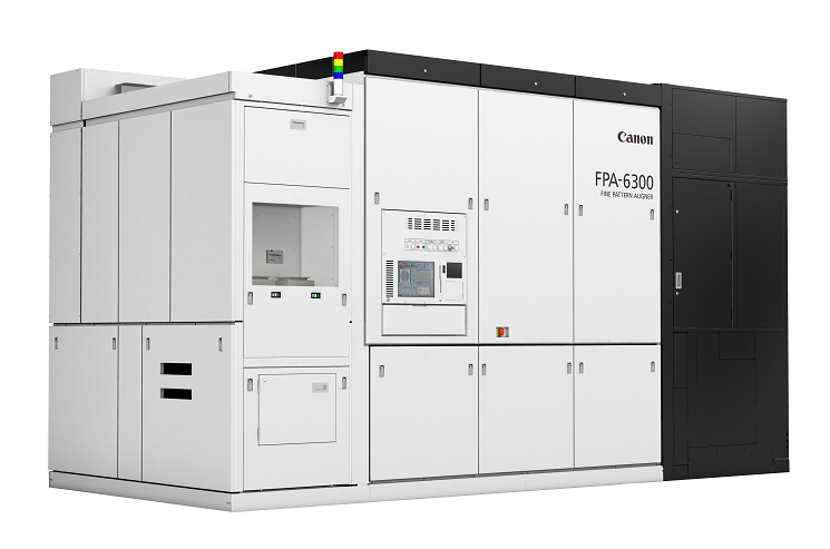
Semiconductor chips are essential components in countless products that support the conveniences of modern life, such as smartphones, computers, home appliances, and automobiles. These chips are manufactured by imprinting circuit patterns onto silicon sheets called wafers through a process known as exposure, in which a photosensitive material is applied to the wafer and the pattern is projected using light—much like how an analog camera exposes film to create a photograph. Semiconductor lithography equipment, one of Canon’s flagship offerings, is used to perform this exposure process.
Although the underlying mechanism is similar to a camera, semiconductor lithography systems require precision on a far greater scale. To imprint circuit patterns with line widths at the nanometer*1 level, the system combines more than a dozen massive lenses—each measuring up to 30 centimeters in diameter— and controls them with micrometer*2-level accuracy (equivalent to about 1/100 the thickness of a human hair).
- *1 One-billionth of a meter
- *2 One-millionth of a meter
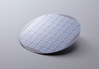
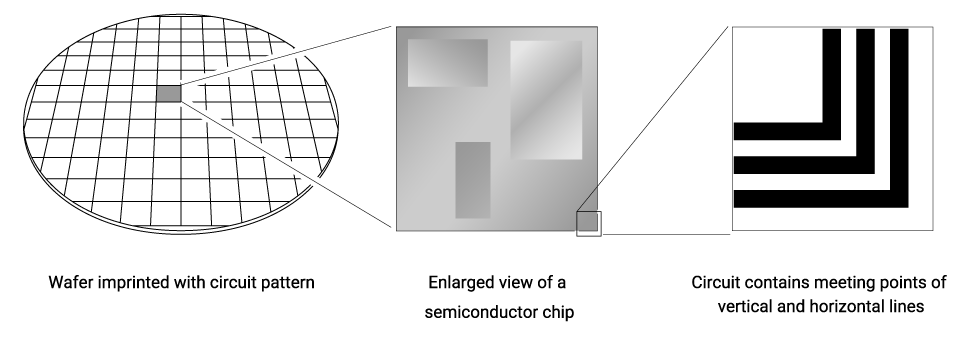
A single wafer typically yields dozens of semiconductor chips, each of which is assembled from multiple circuit layers. The circuit pattern for each layer is imprinted through exposure to light. To form a single layer, the lithography system repeats the exposure process as many times as the number of chips on the wafer. This is where the temperature of the lens becomes critical. Repeated light exposure accumulates enormous energy in the lens, causing it to heat up—which in turn results in deterioration of the lens’ optical precision. Since this process is repeated for each of the many layers until the chip is completed, the cumulative impact of heat becomes a major challenge.

Each circuit layer consists of numerous vertical and horizontal lines, which are typically exposed simultaneously.
To ensure consistent chip quality, Canon has traditionally controlled lens temperature based on calculations of temperature changes from simultaneous exposure of both vertical and horizontal lines.
Uneven heat? Instead of cooling down, try warming it all up!
Despite these measures to control heat, Canon received feedback from users of its lithography systems, who reported that they had to halt production to cool down the equipment because overheating in the lens was reducing exposure accuracy. The root cause lay in a usage method Canon had not anticipated.
In the chip manufacturer’s production line, to improve the precision of the shape of junctions where vertical and horizontal lines meet at right angles, they performed separate exposures for vertical lines and horizontal lines instead of exposing them simultaneously.
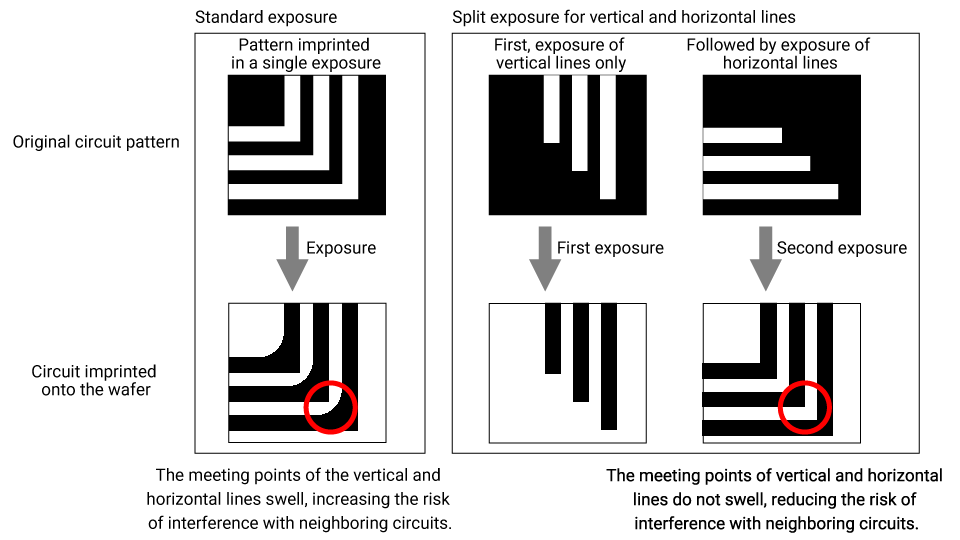
This approach doubled the number of exposures compared to simultaneous exposure. As a result, more energy accumulated in the lens than expected which, in particular, caused its central area to heat up and the heat to linger—a new problem that had not been foreseen.
They thought hard about how to address localized overheating in the lens.
The most obvious solution to restore a uniform temperature across the lens is to cool it down. Due to the material properties, however, heating the lens is easy, but cooling it requires a significant amount of time and energy. Moreover, repeated cycles of heating and cooling can cause microscopic distortions in the lens.
Instead of cooling, the development team came up with a different idea: heat the surrounding areas to match the overheated center’s temperature, thereby equalizing the temperature across the entire lens.
What turned this seemingly radical idea into a viable solution was Canon’s confidence in its proprietary technologies which led to hypotheses such as “We can heat the lens selectively and locally,” and “As long as the temperature is uniform, we can maintain lens performance even at high temperatures.” Combined with Canon’s culture of openly embracing challenges, this approach became a practical solution.
Repurposing the stopper: A ray of hope for putting the radical idea into practice
The team explored ways to heat the entire lens evenly.
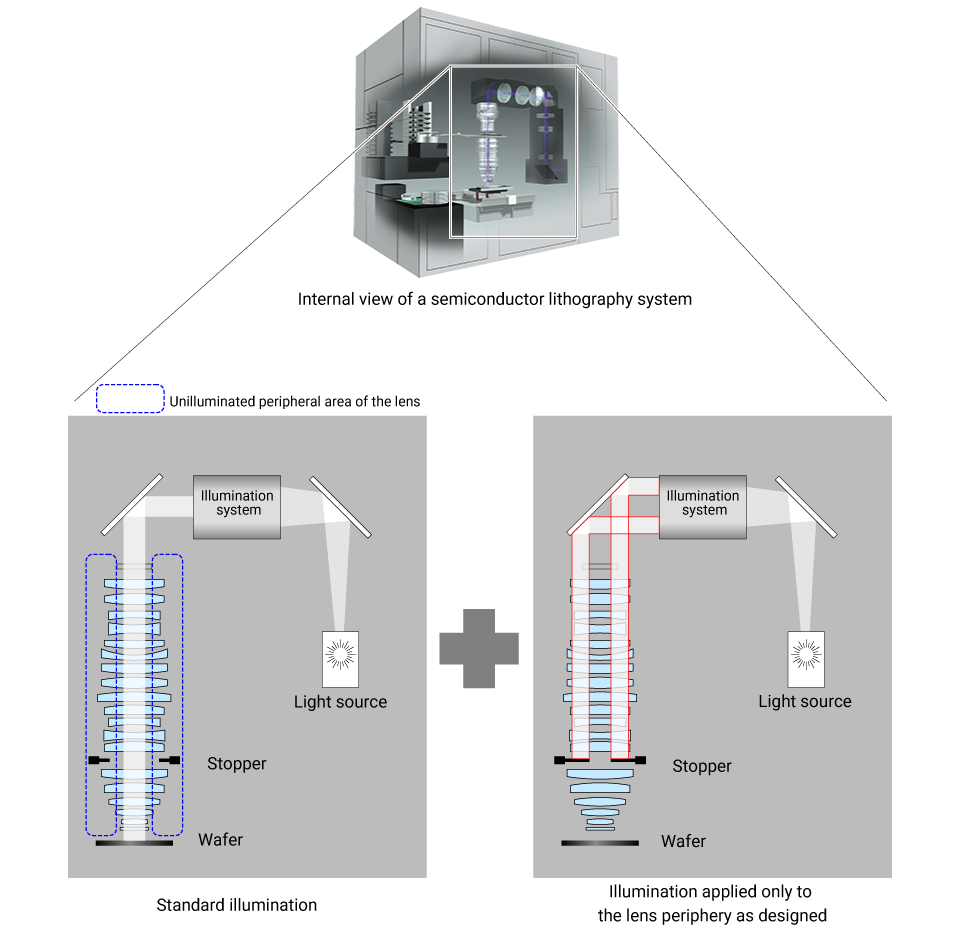
Eventually, they devised a method: immediately after normal exposure—where light is used to imprint circuit patterns onto the wafer—they would shine additional light only on the areas of the lens periphery that had not been exposed during the normal exposure. This would help equalize the temperature between the lens center and its edges. However, since the wafer under the lens is coated with a photosensitive material, this extra light must never reach it.
To prevent this, they focused on a mechanism called the “stopper,” which shapes the light before it reaches the wafer.
The stopper is an adjustable mechanism, similar to a camera aperture. Heat tends to accumulate in the lens group above the stopper, closer to the light source. By closing the stopper and directing light toward the lens periphery, they could effectively heat the peripheral areas of the lens group. Conveniently, the lenses below the stopper are farther from the light source, where light intensity is weaker, so they do not require additional heating (see chart on right below).However, using the stopper in this way meant it would need to withstand intense light across its entire surface—something the stopper was never designed to handle.
Quality matters most for equipment built to last
“Will the stopper maintain its durability and performance even after repeated exposure to intense light?”
When repurposing the stopper—originally designed for a different function in lithography systems—for this new application, its quality had to be revalidated from scratch. Semiconductor lithography systems are extremely expensive and are expected to remain in operation for several decades once installed. Therefore, ensuring durability and performance required testing under conditions equivalent to decades of light exposure.
Canon conducted tests using light far more intense than the actual light source used in production. For several months, they meticulously monitored changes in the stopper’s material properties and functionality on a daily basis, persistently verifying its durability and performance. Eventually, the stopper passed these rigorous tests, enabling it to maintain a uniform lens temperature while supporting specialized applications in manufacturing.
Later, it became clear that many semiconductor manufacturers faced similar challenges. Today, Canon’s lithography systems equipped with this technology are being adopted across numerous semiconductor production sites.
Our modern lives increasingly depend on the evolution of semiconductor chips. For that reason, Canon remains committed to addressing emerging needs and challenges in semiconductor production with integrity, striving to contribute to a richer and more advanced way of life.
Publication date of this article:January 22, 2026
List of Content
Maintaining Trust in the Canon Brand
Vol.11

Vol.10

Vol.9

Vol.8

Vol.7

Vol.6

Vol.5

Vol.4

Vol.3

Vol.2

Vol.1

Canon QA Activities
Quality Management at Canon

Safety Program

Security Measures