Current status of new industry-oriented business group structure
Industrial Group

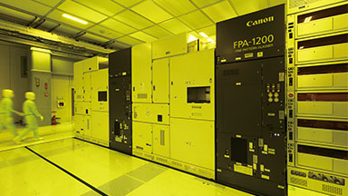
Canon Flat Panel Display (FPD) lithography equipment exposes circuit patterns on glass substrates

Boosting productivity and moving further ahead to advance digital technology

Semiconductor lithography equipment serves to support society

AI, IoT, robotics, autonomous driving, space exploration, and other technologies that will power the future would not be possible without the semiconductor lithography equipment that exposes minute circuit patterns on semiconductor chips.
Canon developed Japan's first semiconductor lithography equipment in 1970. Since then, Canon has introduced many innovative products that both advance semiconductor technology and serve the needs of semiconductor manufacturers to improve productivity.
Today, Canon's lithography equipment utilizing i-line (mercury) and KrF (krypton fluoride) as a light source produces a wide range of semiconductor devices including logic and memory chips, 5G devices, and power devices for automobiles. Canon is committed to offering a diverse range of semiconductor lithography equipment as well as high-quality service.

i-line stepper used to manufacture power devices, image sensors and more

FPD lithography equipment produces beautiful displays

Canon is a leader in LCD and OLED display production equipment. Canon Flat Panel Display (FPD) lithography equipment, which exposes circuit patterns on large glass substrates, is used not only for the manufacture of smartphone displays, but also for large and high-resolution flat-panel displays for 4K and 8K televisions.

Contributing to the commercialization of OLED displays

Lauded for producing deep shades of black, OLED displays offer many more advantages, including energy savings and thin, lightweight designs. Today, OLED is a leading display technology for smartphones, tablets and televisions. Despite its many advantages, OLED technology was slow to catch on due to the difficulty of manufacturing the displays.
Canon Tokki was the first company to commercialize OLED mass production equipment. Since then, they have worked to expand OLED accessibility while pursuing new manufacturing methods and new materials at the vanguard of the industry.

OLED panel manufacturing equipment produced by Canon Tokki

United as one Group in pursuit of new innovations

Through stronger collaborations among Group companies that deal in industrial equipment, Canon is working to expand its business. In addition to Canon Tokki, the Group companies include Canon ANELVA, which produces sputtering equipment using vacuum film deposition technology to form thin metal film for hard disks and DRAMs; and Canon Machinery, which produces die bonders and labor-saving automation equipment. By integrating their respective technologies, these three companies are at the forefront of innovations that will support the next era of manufacturing.

Canon ANELVA’s sputtering equipment deposits uniform nanoscale film under vacuum

Canon Machinery’s die bonder used to attach semiconductor chips

Nanoimprint lithography enables low-cost manufacturing of cutting-edge chips

The miniaturization of semiconductor circuit width continues to progress. Today, attaining an industry-leading line width of under 20 nm requires a massive investment in equipment. Canon's nanoimprint lithography equipment holds great promise as a solution. Pressing nanometer-scale patterns onto the substrate, like a stamp to form minute circuits, Canon's technology holds the promise of huge cost reductions and energy savings.
Now that the equipment's primary performance criteria have been achieved, the next stage is mass production. Currently, Canon is working with semiconductor manufacturers to verify its operation for mass production. Meanwhile, the New Energy and Industrial Technology Development Organization (NEDO) has selected Canon's technology as part of a subsidized project for developing advanced logic manufacturing process applications.

1. Inkjet technology is used to dispense droplets of liquid resin to the wafer surface in accordance with the circuit pattern

2. A mold, or mask, has circuit patterns that are pressed like a stamp onto the resin that has been applied to the wafer surface

3. Ultraviolet light is used to solidify the resin and form the circuit patterns, after which the mask is removed from the resin

Industrial Group main products:
Semiconductor lithography equipment / Flat panel display (FPD) lithography equipment / OLED Display Manufacturing Equipment / Vacuum thin-film deposition equipment / Die bonders / Handy terminals / Document scanners and more

Current status of new industry-oriented business group structure

Society realized by four new businesses that are responsible for a grand strategic transformation